Ive got 3 flash chips with “Serial Flash Discoverable Parameter (SFDP)” tables, a standard way of determining the properties of a chip. I guess it is helpful to determine how to read and program a chip (capacity, block size, etc).
Honestly, it is not something I’ve worked with before and I’m pretty excited.
I have three chips on breakout boards (but I’m also thirsting after a SOIC ZIF socket). Two variants from Puya, and the same Winbond chip that is used in the Bus Pirate.
SPI> [0x9f r:3]
CS Enabled
TX: 0x9F
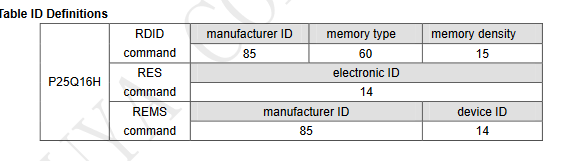
RX: 0x85 0x60 0x15
CS Disabled
SPI>
Most flash chips support 0x9f ID command.There’s also a legacy 90 command.
This is the Puya chip. The output matches the first line.
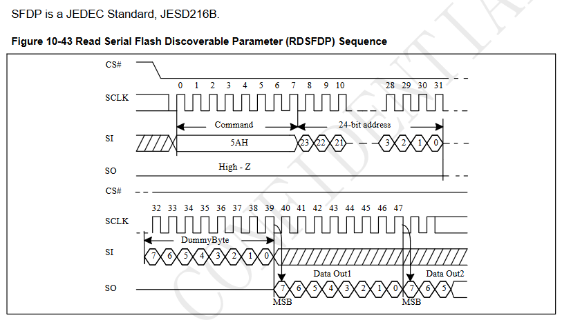
0x5a is the SFDP command. In this chip the table is 0x68 bytes long, and the three byte address sent after the command determines where in the table we start reading.
SPI> [0x5a 0x00:4 r:0x68]
CS Enabled
TX: 0x5A 0x00 0x00 0x00 0x00
RX: 0x53 0x46 0x44 0x50 0x00 0x01 0x01 0xFF
0x00 0x00 0x01 0x09 0x30 0x00 0x00 0xFF
0x85 0x00 0x01 0x03 0x60 0x00 0x00 0xFF
0xFF 0xFF 0xFF 0xFF 0xFF 0xFF 0xFF 0xFF
0xFF 0xFF 0xFF 0xFF 0xFF 0xFF 0xFF 0xFF
0xFF 0xFF 0xFF 0xFF 0xFF 0xFF 0xFF 0xFF
0xE5 0x20 0xF1 0xFF 0xFF 0xFF 0xFF 0x00
0x44 0xEB 0x08 0x6B 0x08 0x3B 0x80 0xBB
0xEE 0xFF 0xFF 0xFF 0xFF 0xFF 0x00 0xFF
0xFF 0xFF 0x00 0xFF 0x0C 0x20 0x0F 0x52
0x10 0xD8 0x08 0x81 0xFF 0xFF 0xFF 0xFF
0xFF 0xFF 0xFF 0xFF 0xFF 0xFF 0xFF 0xFF
0x00 0x36 0x50 0x16 0x9E 0xF9 0x77 0x64
CS Disabled
And there’s the table data. Easy-peas (thanks autocorrect!).
0x53 0x46 0x44 0x50
There’s the signature, big-endian format.
0x00 0x01 0x01 0xFF
Some info
- Minor revision: 0x00
- Major revision 0x01
- parameter headers: 0x01
- 0xff (assume end of header marker)
0x00 0x00 0x01 0x09 0x30 0x00 0x00 0xFF
Location of a table:
- JEDEC header # 0x00
- Minor: 0x00
- Major: 0x01
- Length: 0x09 (in Dwords, so
18 bytes?4*9=36) - Parameter table starts at 00 00 30
- 0xff End of header marker?
0x85 0x00 0x01 0x03 0x60 0x00 0x00 0xFF
Another table location (manuf?):
- manuf ID: 0x85 (I downloaded a list, there is a continuation code I don’t understand at this point)
- version = 01 00
- another param table length 03 =
6 bytes?3 * 4 = 12 - Where is it? 00 00 06
- 0xff end marker
0xFF 0xFF 0xFF 0xFF 0xFF 0xFF 0xFF 0xFF
0xFF 0xFF 0xFF 0xFF 0xFF 0xFF 0xFF 0xFF
0xFF 0xFF 0xFF 0xFF 0xFF 0xFF 0xFF 0xFF
Looks to be 24 bytes of 0xff?