Still in the snailmail as it seems…
2 Likes
can’t edit. came just before last chance for before-38c3-delivery
1 Like
I’m so glad it arrived in time! Let us know what you think.
Hey @ian, I love the idea! Is there any possibility of modifying it and adding female pins on the other end? That way, we can create a system of plugins/chains and make boards that can connect to each other according to requirements, with different functionalities—male → ← female → male …
2 Likes
Sure, I started with a design with more stuff, but then backed off to get a usable prototype.
2 Likes
I am so bad at soldering blank plank. Will try to lower temp to get prototype to test and if it works then own PCB (plank). It will be my first and simple but should do the work. If it works
2 Likes
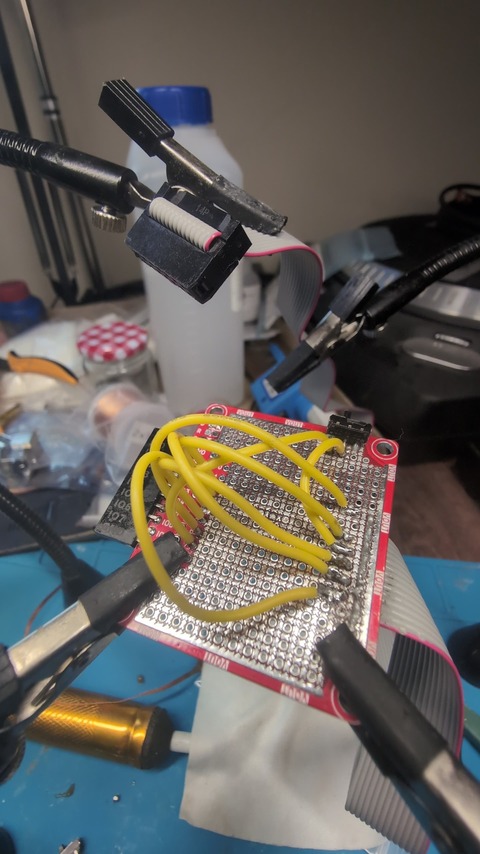

It ain’t pretty but it’s honest work🤣 Bridging connections was pain. Lot of flux to solder. Then clean from flux and lower temp to bridge. But verified connections and it should work.
Edit:
BTW its silicone coated cable. Since I got this type with BP5 there is no comming back. Silicone soft and nice!
3 Likes
I think it looks good! Thank you for testing dirtyJTAG. My JTAG test targets are still in the mail.
1 Like
I added one to a recent order, so I ended up with two, which both arrived recently. Here’s my initial thoughts (#1-4), of which two have feedback (#1, #4), and conclusion. Wrapped in details to reduce scrolling in thread later.
click to expand
Thoughts #1:
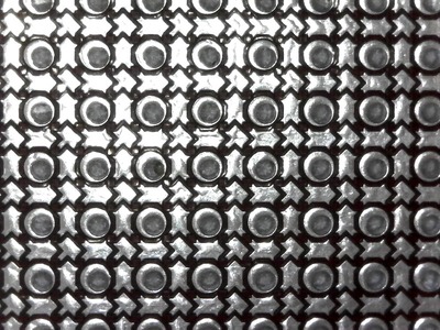
The drilled holes are not centered in the inner ring (but always are still in them, even if touching an edge). Normally, the tolerances aren’t that big a deal. However, when soldering PTH components (even a resistor), having an essentially non-existent ring on one side of the pin does makes it hard to avoid soldering to ground. Yes, lots of flux helps (likely because the ground plane is large and thus relatively cool), etc. Note that this is not as critical on the front side, since the solder is only flowing through the board from the back side for the PTH components.
Feedback #1:
Maybe increase size of “inner” ring around these holes, or have made on
at a production line that provides tighter tolerances / alignment?
NOTE: Green prototype drill holes were all very tight tolerance?
Thoughts #2:
The header was perfectly spaced to align with the board edge. Nice!
Thoughts #3:
I spent a bit more time than expected trying to find a way to solder the first header pin. This was primarily because half the header height overlaps the board, so I couldn’t just put other temporary headers under the other side of the board. So, I had to find a spacer that was just the right height.
Thoughts #4:
The header will have more force applied to solder joints during insertion / removal. I applied solder to both the top and bottom to increase the joint strength. I noticed that the leads of the header lay on top of the board … but above a solder masked portion. Thus, the strength of this joint is only provided by the 90 degree-offset PTHs.
Feedback #4:
On the top of the board, from the header holes to the nearby edge, add extra-thick traces (and remove the red solder mask … essentially adding extra pads). This would allow application of additional solder on the horizontal portion of the header leads, giving a large surface area and thus stronger anchor, if folks desire to solder that portion down. If I wanted to keep a board after prototyping, I’ll likely epoxy the joint … but being able to have the extra solder joint would be nice.
Overall / Conclusion
If I knew the final layout of the circuit, and didn’t have a breakout for SMD components, I would use this board.
If I had more SMD parts, I would definitely keep some of these around, especially for quick prototypes.
At the same time, I’ll still prefer to use SMD breakouts (to 0.1" spacing), and just attach the breakouts to breadboards, and then to classic protoboards.
2 Likes
Some additional pad to secure the 10P is a nice idea.
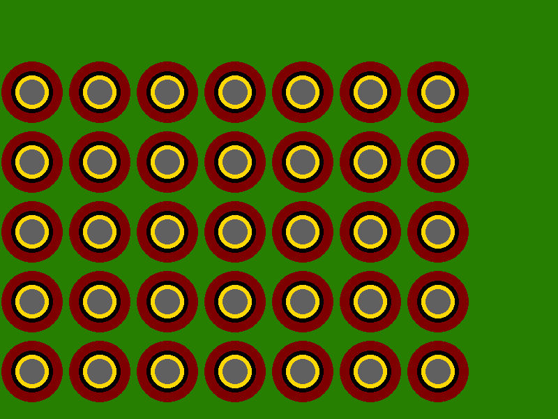
On the green board I think the holes look pretty centered. I don’t have a red board yet though, my last shipment of stuff seems to be stuck somewhere.
2 Likes
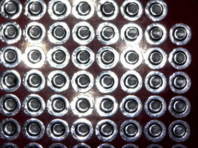
Here’s two closeups, taken using a Plugable microscope.
You can see that many of the holes come quite close to hitting the outer ground ring. It’s very likely within specified tolerances … just that this type of board may need tighter tolerances.
5 Likes
Uhh, that looks bad.
Yes, this design needs better tolerances to squeeze all the features into the 2.54mm pitch.
2 Likes
Oh yeah, that looks terrible, thank you for the photo. I’ll have more made up and sent out.
2 Likes
I was thinking about this more, I wonder there might be a better option for the back…
Color Definitions
- Grey – pass-through hole
- Gold – pass-through hole solder ring
- Dark Red / Brown – Solderable Ground pad
- Black – No solder mask, no copper (solder jumperable)
- Green – Solder mask
- White – Print layer
- Pink – Solderable
VINpad
Old back had very small rings around the pass-through holes to have the “solder volcano” sit. This therefore required tighter tolerances with drill placement:
For the new back, use standard through-hole pads, so soldering is a breeze and drill tolerances don’t need tightening. Then, rather than a single larger ground pad, have a gap (black ring) and four solderable corner pads … allowing the same “bridging” technique as used on top to ground the PTH. Even better … run VIN to some of the pads.
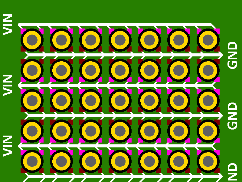
The four pads around each standard PTH pad … may as well make them similar to PTH GND solder pads … where the pad has smaller connectivity to the larger ground plane / VIN trace. (I think this lets the soldering iron heat the little pad, thus solder to ground more easily?) Here’s a close-up of this thought… notice the black lines mostly around each of those corner pads.

Oh, and obviously, VIN would need to be routed (e.g., under the corresponding silkscreen) to the VIN pads.
Thoughts?
3 Likes
I like the idea.
Just touching the edges to connect is something that could make not accidently connecting GND easier.
Regarding the bigger ring - this will probably require some kicad hacks, because you can’t increase the ring on the top without violating the DRC there. I don’t think kicad supports different ring sizes on the two sides out of the box. Also the top side is why you still need some better drill tolerances from your fab. So I suggest to not overdo increasing the ring size. I think this is something that has to be fixed more on the fab side and less on the design side.
Regarding Vin - If you route Vin like every second row to make this possible, you get very wide ground return paths. So it will work for simple circuits, but it won’t work well for analog or faster digital. I initially designed this ground plane option to improve ground connections for these cases. But in practice I found it also quite convenient for other cases, that is why I suggested to use this pattern here.
For prototyping the Vin-routing could be a very valid compromise though. Would make routing Vin much easier. So maybe offer two versions?
2 Likes
On the top side, even if the drill is just barely within the pad, wouldn’t that be “good enough”?
I’m a hack … your expertise is why I’d ask here. If I understand you correctly, break the ground plane into columns with thin VIN traces causes problems with analog / faster digital signals. I’m ignorant here … is there a term of art that I could search, to find tutorials that might help me understand the problems this causes? Maybe having a limited number of VIN pads would help (e.g., small branches from outer edge only … not all the way across) … after all, VIN isn’t needed everywhere, and is also available up top. Might also find provide a nice way to spread VIN to the top also
3 Likes
Consider you don’t want to use this hole for mounting some THT part, but for routing a signal through with solder blobs. It will work, but it is more difficult to make the solder connection.
Maybe “PCB trace impedance” as a search term?
Current always flows in current loops. So when you set a digital signal from low to high, you have some parasitic capacitance and inductance to overcome. Current needs to flow for this. You have the same amount of current as return current to ground in the opposing direction. So far so good.
Now with fast signals the forward and return currents want to stay together on the PCB as close as possible. The more their paths are spaced apart, the more energy is required for this and the more energy is emitted as EMI.
Also when you open such a loop area up, the trace path becomes more susceptible to EMI from other parts or devices. This is why this also matters for precision analog stuff, even if you don’t have fast signals there.
So when you have the Vin trace going to the center of the pcb, it could require the return current to flow all the way to the outer edge and then back.
But to put this into perspective, this is all still far far better than when you use a traditional breadboard. Because the breadboard doesn’t just add instable connections, but also huge parasitic capacitance and inductance due to all the springs and wires.
I’m not sure if having Vin just on the outer rows is a good compromise. It would require the user to much more plan than they already have to.
I think offering two different versions is the better idea. You grab the Vin version for your regular and simple circuits and the gnd-only version for when you do high-speed or precision analog stuff.
3 Likes
Dumb question - What if the Vin rails weren’t connected? You add a “jumper” connecting a rail to the side rail? Or have a choice of two “jumpers”, so you can make a rail either Vin or GND?
3 Likes
This has been a nice discussion. I really like the dual VOUT/GND rails, and it might be a bit more friendly for soldering than a double ring. The ground return would be atrocious though… 4 layers won’t help unless we do buried vias but I think that is out of the range of a protoboard. I like the direction this is going though.
My green prototype boards have perfect drills, I have no idea why the black boards were so sloppy. I’m going to mail everyone a green board snail mail from here in NL.
2 Likes
I was going to add a couple of these to an order, but once it’s in my cart, it says “Back Order Not Available (0 in stock)” – are they really out, or is this normal?
2 Likes