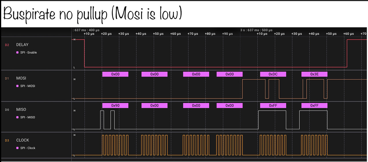
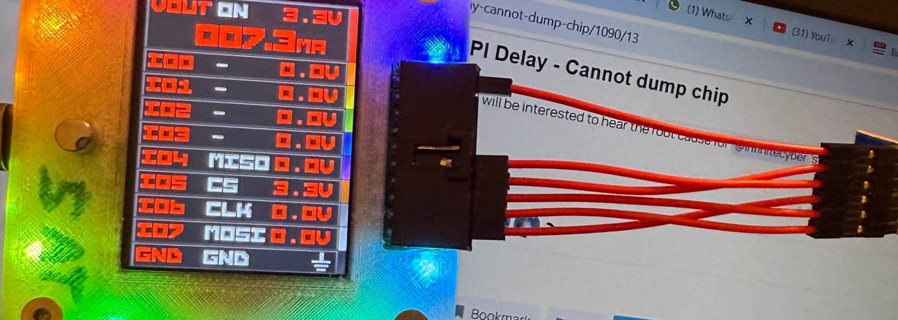
After each byte, there is a small delay of 6-8 us in the buspirate. Unfortunately this seems to make a huge difference. I am not able interact with the chip at all.
I followed along the exact same instructions out of the tutorial.
HiZ> m

Mode selection
1. HiZ
2. 1-WIRE
3. UART
4. I2C
5. SPI
6. LED
x. Exit
Mode > 5

SPI speed
1 to 62500KHz
x. Exit
KHz (100KHz*) >
Data bits
4 to 8 bits
x. Exit
Bits (8*) >
Clock polarity
1. Idle LOW*
2. Idle HIGH
x. Exit
Polarity (1) >
Clock phase
1. LEADING edge*
2. TRAILING edge
x. Exit
Phase (1) >
Chip select
1. Active HIGH (CS)
2. Active LOW (/CS)*
x. Exit
CS (2) >
Actual speed: 122KHz
Mode: SPI
SPI> W
Power supply
Volts (0.80V-5.00V)
x to exit (3.30) >
3.30V requested, closest value: 3.30V
Set current limit?
y

Maximum current (0mA-500mA)
x to exit (100.00) > 50
50.0mA requested, closest value: 50.0mA

Power supply:Enabled

Vreg output: 3.3V, Vref/Vout pin: 3.3V, Current sense: 5.8mA

SPI>
I also enabled pull up resistors and disabled it:
SPI> P
Pull-up resistors: Enabled (10K ohms @ 3.3V)
SPI>
I did sent the command with a reset before and without:
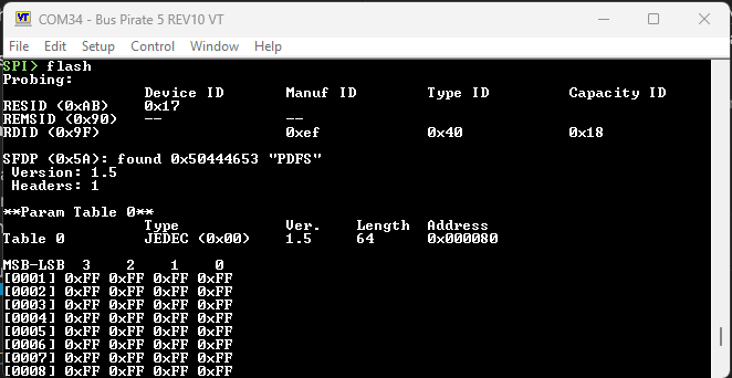
SPI> [0xb9] D:10 [0x90 0x00:3 r:2]
SPI> [0x90 0x00:3 r:2]
and so on...
This also affects all other commands. I also tried using the “flash init” command and also the binmode together with flashrom. The chip is not being recognized. Even if I try to dump it out of circuit. I compared multiple comands against a different board that was able to dump the chip and the only difference is the delay as shown above. Is it possible to get rid off it?
If you need more / better logs, please just let me know but I guess the issue is tied to the delay of the SPI command.
PS: I really like the buspirate 5 and would like to use it in my upcoming trainings
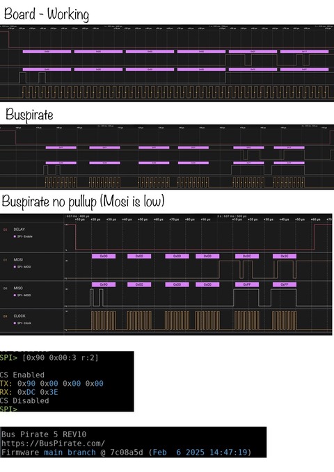
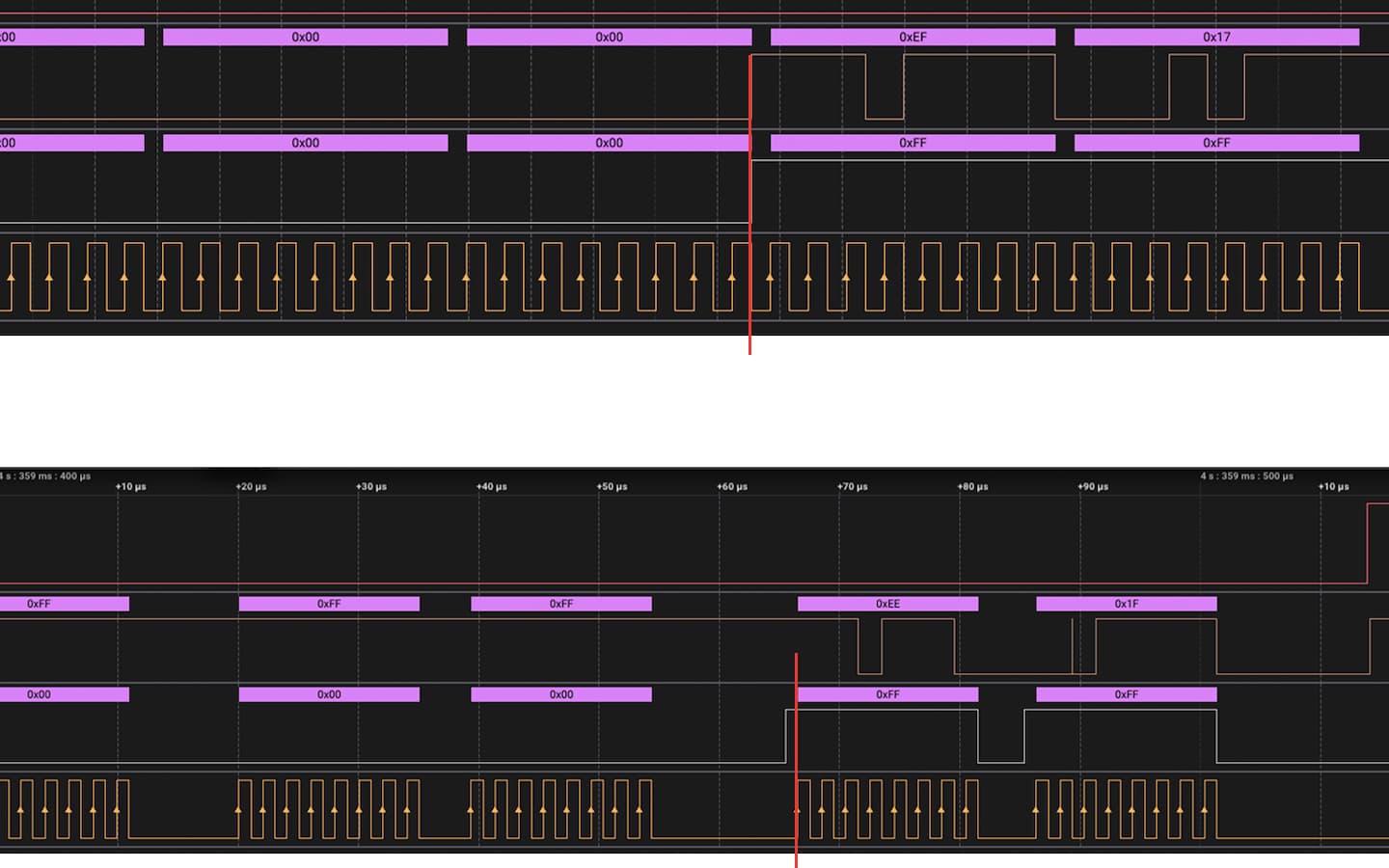
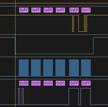
The first signal is from a board that is getting back the correct value (0xef 0x17). The second picture is from the bus pirate. One difference is the brown line (pull-up) but I also tried it without pull up then all lines are identical beside the delay in the buspirate which seems to cause the different result. (0xee 0x1f)
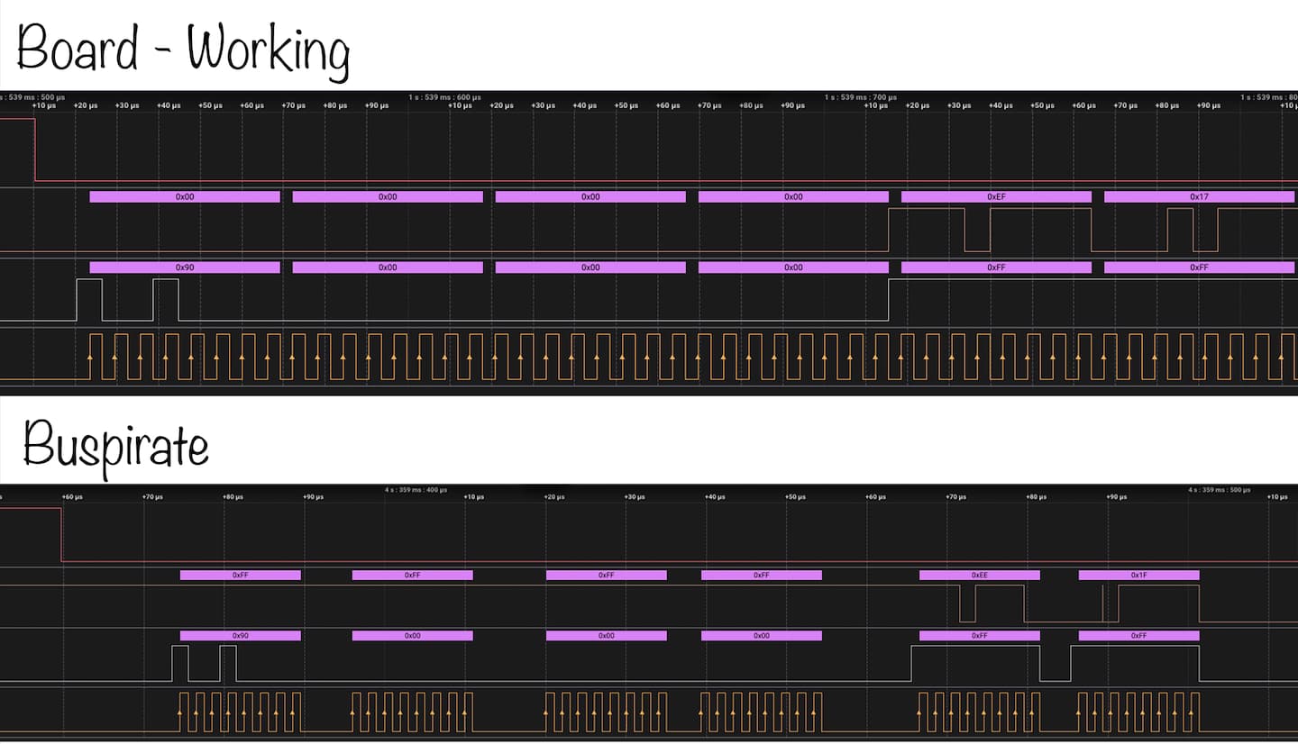
This is how it looks like if the Pull-Up is not being set. I guess it is a better comparison to the working board. Unfortunately still a different decoded value. Not just in my salae logic analyzer, also in the buspirate.
Thank you so much for the detailed analysis. I’m sorry about the issue.
I have never seen between byte delays cause read errors on common flash made in the last 20 years. It is totally possible, but I suspect another issue.
Are the write protect and hold pins connected and held high? That is the purpose of enabling pull ups, to disable those functions. Can you do a logic capture that includes write protect and hold?
What is weird is that the bus pirate sends the right command, it is the chip that doesn’t respond correctly. So I doubt it’s a WP or HOLD issue, but I’ve never tested with those pins floating.
I have this chip and will test for firmware bugs or regressions, but I won’t be able to test for another 12 hours or so. The data sheet would also specify a max time between bytes, I’ll check that now.
I checked the data sheet and I didn’t see a maximum time between bytes. The chips are designed to be suspended when the HOLD pin goes low for as long as needed, so basically unlimited between byte time.
Will test a chip asap.
How are you set up? Using a plank with a socket? Probing on a breadboard?
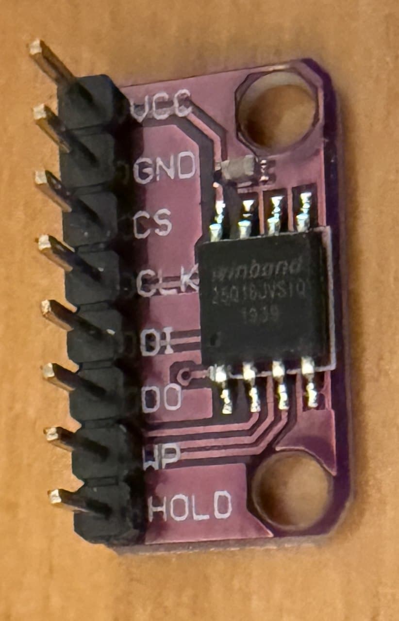
I also am trying to read a standard Winbond WQ flash using the SOP8 adapter. I tried a few days ago and had issues, and thought it was just me, and didn’t have time for even basic troubleshooting.
Trying it now (I’ll add comments with #):
# SPI @ 100kHz, 8 / Idle Low / Leading / Active Low
HiZ> m spi

Mode: SPI

Use previous settings?
 SPI speed: 100 kHz
 Data bits: 8
 Clock polarity: Idle LOW
 Clock phase: LEADING edge
 Chip select: Active LOW (/CS)

y/n, x to exit (Y) >

Actual speed: 99kHz

# I enabled pull-ups before power ... but no change either way
SPI> P


Pull-up resistors: Enabled (10K ohms @ 0.0V)
Warning: no/low voltage detected.
Enable power supply (W) or attach external supply to Vout/Vref

# Set to 3.3V
SPI> W 3.3
3.30V requested, closest value: 3.30V
Current limit:Disabled

Power supply:Enabled
Vreg output: 3.3V, Vref/Vout pin: 3.3V, Current: 3.0mA

# Send the reset, delay 10ms, read ID commands
SPI> [0xb9] D:10 [0x90 0x00:3 r:2]

CS Enabled
TX: 0xB9
CS Disabled
Delay: 10ms
CS Enabled
TX: 0x90 0x00 0x00 0x00
RX: 0xFF 0xFF
CS Disabled


# Disable pull-ups and try again
SPI> p
Pull-up resistors: Disabled

SPI> [0xb9] D:10 [0x90 0x00:3 r:2]

CS Enabled
TX: 0xB9
CS Disabled
Delay: 10ms
CS Enabled
TX: 0x90 0x00 0x00 0x00
RX: 0x00 0x00
CS Disabled
OK, without pull-ups, it fails because the plank’s HOLD and WP lines (IO2 and IO3) drop to 0V. Override those to be high:
SPI> ?
# ... trimmed ...
send and receive data in modes using bus syntax
# ... trimmed ...
a/A/@.x Set IO.x state (low/HI/READ)
v.x     Measure volts on IO.x
>       Run bus syntax

SPI> p
Pull-up resistors: Disabled

SPI> > A.3 A.2

IO3 set to OUTPUT: 0
IO2 set to OUTPUT: 0
So, it seems I cannot currently tests without pull-ups enabled, as I clearly cannot read the built-in help correctly; I appear to be unable to override IO2 and IO3 to output high?
Note: I’m using firmware ci-buspirate-main-1a34626.zip from 2025-03-16.
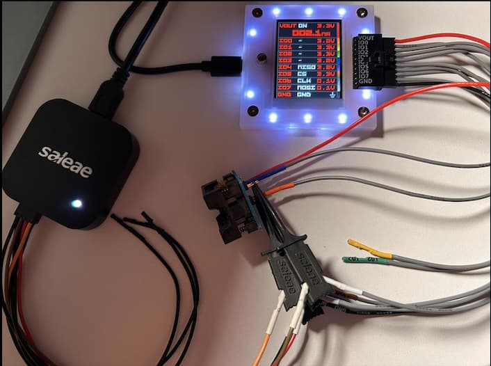
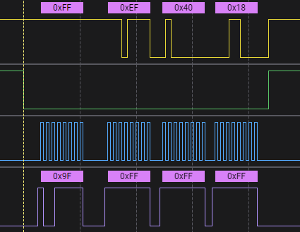
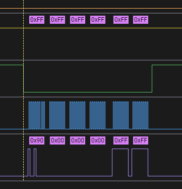
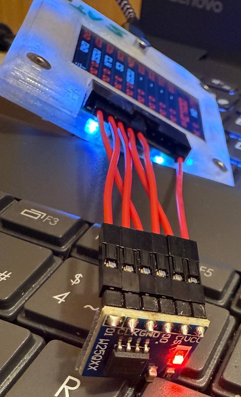
Thanks for the fast reply!! I tested it with the Pull-UP connected to the WP / Hold. As you mentioned, it does not change the behaviour. I am using an adapter shown below:
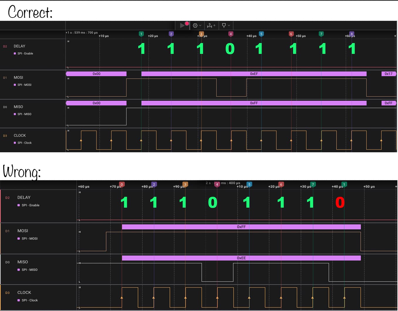
The above picture is correct and it aligns with MISO/MOSI and at the bottom is the signal of the buspirate.Maybe the clock is kicking in one cycle too late? But the rising edge fits, so not sure. I will decode it manually and verify it
Hm ok yes. It looks like we are off one clock cycle. Therefore also the logic analyzer is displaying it “wrong” because the clock will be provided by the bus pirate - one cycle too late? I try to play around with this behaviour a bit and thanks for looking into it. It is not time critical to me! You can also enjoy your weekend
I am still not 100% sure where the issue is but I hope this helps in investigating. As already mentioned. Thanks for diving into the topic and debugging it. I really like this project and I appreciate the time and effort you put into it It is not time critical and I do not expect you to put this on the top of your agenda ^^. Take your time and if it can be resolved, fine Thanks!
I think I have a Winbond 25Q128 chip lying around—I’ll do some tests tonight.
I haven’t read the whole thread in depth yet, but just to rule out common issues… @infinitecyber
Can you try using very short Dupont cables, without the original Bus Pirate cable?
Don’t connect a logic analyzer or anything—just very short Dupont wires, and double-check that everything is properly connected. Also, connect the WP and HOLD pins of the chip directly to 3.3V via 10K or 4k7 resistor, and try again. Let me know if anything changes.
Have you used that specific Bus Pirate + cable for other things successfully in the past, or is it brand new?
I’ll run some tests tonight with the latest firmware and my Bus Pirate v5, and I’ll let you know what I find…
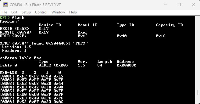
Now it works consistently. The issue for me was power supply. I use a prototype version of the SOP flash adapter, and the power supply label is backwards. I was powering the chip from the pull-up resistor on IO0 instead of the actual power supply.
Once I connected the chip to a solid power supply it responds to all ID commands and the SFDP info is readable.
Is it possible the power or ground connection between the Bus Pirate and chip is weak/disconnected? Is it possible the chip is being back powered through a pin?
Are MOSI/MISO swapped in the correct vs wrong traces above? And these are both replies from the chip right? Unless there is a physical short or damage, an SPI master (the bus pirate) should not generally be able to induce an off-by-one bit error in sub device (flash) output. You would see the missing clock ticks and your analyzer wouldn’t decode it correctly.
I suspect this is a power issue. I can confirm that the firmware you’re using can correctly read and write these commands when the chip is properly powered.
I then got it working … and it was, as you thought, a power problem. I feel a bit silly, but in case others have trouble, the following allows the plank to work regardless of pullup / plank switch settings:
> A.0 a.1 A.2 A.3
IO0 is set high (VCC_PIN @ 3V3, so plank switch won’t matter)
IO1 is set low (GND_PIN @ 0V, so plank switch won’t matter)
IO2 is set high (HLD @ 3V3, should it be labeled/HLD??)
IO3 is set high (WP @ 3V3, just to prevent floating pin … should it be labeled /WP??)
Anyways, the above single line helped for this plank.
Now, I will be interested to hear the root cause for @infinitecyber’s situation…
Hello all! Thank you so much for all the debugging support! I tried different cables and also switched out the adapter. It now works… I am sorry for the trouble you had for such a basic issue. It was a new device and maybe I accidently squeezed a cable. I will use them in my training and order a larger number so hopefully you got a little bit of value back for your time
@henrygab found a major bug in the process so don’t worry, it’s already paid off. Thank you again for the detailed bug report and let me know if you have other issues.
No worries! It’s always good to re-check our stuff, and as Ian noted, your report caused another bug to be found/fixed. Glad to hear you got it working.