Just putting an idea out here that popped into my mind while testing current consumption for changes to the led mode. One test while implementing the changes suggested would be to draw different amount of current from the Vout pin and watch the LEDs get dimmer and dimmer as we prioritize current supplied to devices under test/planks. An adjustable current sink aka dummy load aka active load would be an ideal device to test things out. It’s usually pretty easy to implement, here is a famous example called Re:load. Basically the plank would be similar but instead of manual adjustment with a potentiometer, we can adjust the current draw via the command line or via binary mode.
2 Likes
RE:load is a blast from the past.
The current would be adjusted with PWM through a low pass filter?
1 Like
Exactly. The original design is controlled via a potentiometer, this will be replaced with a PWM input + low pass filter. Here is another example by GreatScottLab that’s closer to what we want.
2 Likes
A I2C current sense chip is one of the breakouts I ordered a few days ago. That might be a nice pairing.
1 Like
It may be, is it INA231 based on Breakout board demos topic?
Re:load is using an op amp as a voltage buffer/comparator circuit to control the MOSFET. It doesn’t have a closed loop control method, I was planning on using the other op amp in the same package to amplify the voltage drop on the resistor and monitor things with an ADC pin, so I would’ve used 2 pins only: one for PWM signal, another for ADC. But with INA231, we can use it for measuring supply voltage as well. There’s an alert pin, automatic power calculation… It’s definitely something to consider.
1 Like
Indeed! Pretty sure I already have some, but I got a few more because most of my breakouts are getting old and a lot of the chips are EOL.
Maybe I will check out that chip tomorrow if the planks don’t arrive.
Let me know how it goes and if you like it or not.
One worry I have with that is the package looks ridiculously small. That’ll make prototyping a bit harder. Or I can use INA219 that has a friendlier package, and the breakout board from Adafruit is available locally. It has programmable gain as well, which may come in handy. One worry is that it’s high side only but that shouldn’t be a problem, we should be able to put the MOSFET between the shunt resistor and ground.
2 Likes
Most of our prototypes are professionally assembled these days, it’s just the most cost efficient way to do it. I keep the szlcsc part numbers in the kicad files, and then the lcsc bom tool does the rest. It goes straight to assembly along with the PCBs.
Shipping all that to me to make one or two prototypes is more expensive than one assembled board in a bubble mailer. I realize the rest of the world hasn’t caught up, JLC isn’t dirt cheap and their system is still limited. But inside China assembly service is as cheap as PCBs became years ago making home etching and drilling just not worth the faf.
Also it’s SOT23, I’m sure you could solder it ![]()
2 Likes
Yeah, I don’t think I want to solder INA231’s chip scale package at home. INA219’s SOIC or SOT23 is easier for me. But the reason I’m thinking about getting the breakout board first is to test a few things before spending any time with creating a prototype board. I already have all the parts required for Re:load at hand somewhere, I was planning to build my own version on a perfboard but then some other stuff took priority. I should be able to do some tests over the weekend then start working on some board designs.
Your time in Shenzhen definitely changed how you approach to things. I have friends here who order barebone PCBs from JLC and parts from Digikey/Aliexpress/Akihabara and assemble all by hand. I think once they did some production for a digital badge but don’t ask me how it went. ![]()
BTW, GitHub - DangerousPrototypes/BusPirate5-hardware: Bus Pirate v5 Hardware is the repo for all the plank designs, right?
2 Likes
Oh yeah, I didn’t see a chip scale package but that is probably a no go ![]()
Yes, all the planks are in the hardware repo. Or should be. I will find some time to clean it up a bit.
2 Likes
Got some INA219 breakout boards off the rainforest shop and they arrived today. I’ll spend the weekend playing around with them. Then I can solidify the current sink plank project.
I wonder what’s a suitable range for people is. I have a huge power resistor and a heatsink I can attach to the MOSFET in my parts bin. I think we should be able to achieve Re:load specs pretty easily. And with the help of adjustable gain setting on INA219, we should be able to have pretty decent resolution at lower current levels.
2 Likes
Let me know if you find the time, I would also like to play along with the INA. I have the older version I believe, I’m looking for it now.
1 Like
I couldn’t find the older breakout, so I had a look at the INA231. The major part seems to be some math to set the calibration value based on the mounted shunt resistor and the expected current limit. I’ll need to make a spreadsheet for that, it’s kind of dense. For now I just programmed the value in the datasheet.
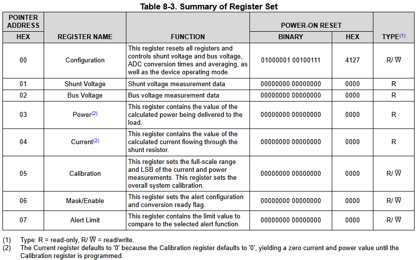
This is the register set. Configuration should be 0x4127, and everything else 0x00.
I2C> [0x80 0 [0x81 r:16]

I2C START
TX: 0x80 ACK
TX: 0 ACK
I2C REPEATED START
TX: 0x81 ACK
RX: 0x41 ACK 0x27 ACK 0xFF ACK 0xFF ACK 0xFF ACK 0xFF ACK 0xFF ACK 0xFF ACK
    0xFF ACK 0xFF ACK 0xFF ACK 0xFF ACK 0xFF ACK 0xFF ACK 0xFF ACK 0xFF NACK

I2C STOP
Configuration looks fine, but everything else is 0xff, even after programming the calibration register. Something seems off.
- It is possible to change the config register, but no other registers respond to changes.
- Noticed a “BUS” pin on the breakout. The datasheet says it should be connected to IN+, but it’s not connected to anything. Powered that, but no change.
AHHHHH, figured it out. You can only read one 16 bit register address at a time.
I2C> [0x80 5[0x81 r:2]

I2C START
TX: 0x80 ACK
TX: 5 ACK
I2C REPEATED START
TX: 0x81 ACK
RX: 0x0A ACK 0x00 NACK
I2C STOP
I2C>
Okay, that’s really dumb. Why can’t I read the whole chip in a single operation?
When reading from the INA231, the last value stored in the register pointer by a write operation determines
which register is read during a read operation. To change the register pointer for a read operation, a new value
must be written to the register pointer
Ah, there we go. It’s so you can take continuous measurements of voltage or current without a write operation before each.
I2C> [0x80 5][0x81 r:2][0x81 r:2][0x81 r:2]

I2C START
TX: 0x80 ACK
TX: 5 ACK
I2C STOP
I2C START
TX: 0x81 ACK
RX: 0x0A ACK 0x00 NACK
I2C STOP
I2C START
TX: 0x81 ACK
RX: 0x0A ACK 0x00 NACK
I2C STOP
I2C START
TX: 0x81 ACK
RX: 0x0A ACK 0x00 NACK
I2C STOP
I2C>
I’m not in a very spreadsheet mood right now, so we can look into that later ![]()
2 Likes
I had some time to do some minimal tests with the INA219 board I got. I’ll try to do some current measurements at some point but I need to do soldering for that (probably). And to do some soldering I have to clean up my workbench, so it may be a while.
I would’ve warned you about the weirdness about read operations, but you figured that and the reason yourself, so kudos to you! ![]()
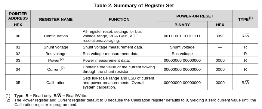
Here are the registers for INA219. So let’s try the configuration for now.
I2C> [0x80 0x00][0x81 r:2]

I2C START
TX: 0x80 ACK 0x00 ACK
I2C STOP
I2C START
TX: 0x81 ACK
RX: 0x39 ACK 0x9F NACK
I2C STOP
As expected, the default configuration is 0x399F. Basically this translates to:
- Bus voltage range: 32 V
- PGA gain: 1/8, ±320 mV range
- Bus and Shunt ADCs: Both 12 bit, 532 us conversion time
- Mode: Shunt and bus, continuous
Now let’s see all the other registers:
I2C> [0x80 0x01][0x81 r:2]

I2C START
TX: 0x80 ACK 0x01 ACK
I2C STOP
I2C START
TX: 0x81 ACK
RX: 0xFF ACK 0xFF NACK
I2C STOP
I2C> [0x80 0x02][0x81 r:2]

I2C START
TX: 0x80 ACK 0x02 ACK
I2C STOP
I2C START
TX: 0x81 ACK
RX: 0x06 ACK 0xD2 NACK
I2C STOP
I2C> [0x80 0x03][0x81 r:2]

I2C START
TX: 0x80 ACK 0x03 ACK
I2C STOP
I2C START
TX: 0x81 ACK
RX: 0x00 ACK 0x00 NACK
I2C STOP
I2C> [0x80 0x04][0x81 r:2]

I2C START
TX: 0x80 ACK 0x04 ACK
I2C STOP
I2C START
TX: 0x81 ACK
RX: 0x00 ACK 0x00 NACK
I2C STOP
I2C> [0x80 0x05][0x81 r:2]

I2C START
TX: 0x80 ACK 0x05 ACK
I2C STOP
I2C START
TX: 0x81 ACK
RX: 0x00 ACK 0x00 NACK
I2C STOP
Both shunt voltage and bus voltage are garbage values as the current measurement section is left floating for now. But power, current and calibration is all 0x0000 as we expected.
2 Likes
TI datasheets do math in a way that I disagree with, so I always have to make the app note or video into a spreadsheet to see exactly what units they’re shifting around without mention. From this TI youtube video.
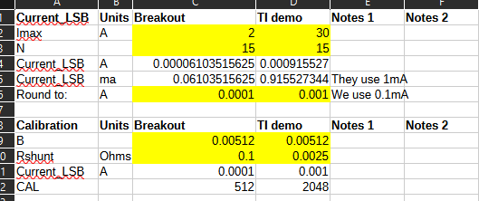
- 2A max current
- 100mOhm shunt resistor
Current LSB: 0.1mA (0.0001A)
CAL: 512 (0x1ff)
- Current is straight forward: current register value * current LSB.
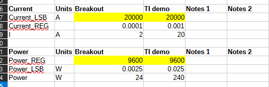
- Power I’m not sure about, we need the power LSB.
The Power register LSB has a fixed ratio to the Current register LSB of 25 W/bit to 1 A/bit. For this example, a programmed Current register LSB of 1 mA/bit results in a Power register LSB of 25 mW/bit. This ratio is internally programmed to make sure that the scaling of the power calculation is within an acceptable range.
I believe the power LSB is calculated from the current LSB. This right here is why I hate IT datasheet math. Show your work, don’t put it in the middle of a massive wordy paragraph!
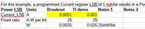
If they use 1mA/bit and get 25mW/bit, I assume with 0.1mA per bit we get 2.5mW/bit
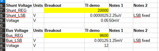
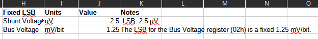
Shunt voltage and Bus voltage are easy because the LSB values appear to be fixed.
Spreadsheet if you’d like to check my work ![]()
ina231.zip (2.8 KB)
1 Like
I got sick and spend the last week in the bed, so not so much progress on this. But here is a link to the INA219 Arduino library from Adafruit: Adafruit_INA219/Adafruit_INA219.cpp at master · adafruit/Adafruit_INA219 · GitHub
In particular they set the calibration value to 3 different values:
Nice thing is they go through the whole calculation and set up the config register as well. Seems pretty straightforward and should be doable in the firmware as well. Or we can pre-calculate some values and give them out as options.
I’ll try to run some tests with these, monitoring the current and power consumption of an LED circuit. That should be a valid test. Maybe we can turn it into a demo as well.
2 Likes