DDR4 SPD read/write adapter

DDR4 SPD plank arrived, and a used SODIMM just fell through the mail slot.

  • The wrong header was soldered
  • Still need to figure out the 9volt supply, probably a 9 volt battery.

SA1 is held high to ground A1 pin, then we can read out the 256 bytes of contents with [0b10100001 r:256].

2 Likes

Set page and address

DDR4 SPD chips typically have 2 pages of 256 bytes each.

  1. Send 0b0110+1100 to set page 0, requires 2 dummy bytes
  2. Send 0b1010+0000 then the address to read from (0x00)
  3. Send 0b1010+0001 then read 256 bytes
  4. Repeat to read page 1

I2C> [0b01101100 0b0 0b0] D:1 [0b10100000 0] D:1 [0b10100001 r:256]
Read page 0.

I2C> [0b01101110 0b0 0b0] D:1 [0b1010000 0] D:1 [0b10100001 r:256]
Read page 1.

Decode a bit

0x23 ACK 0x11 ACK 0x0C ACK 0x03 ACK 0x84 ACK 0x19 ACK 0x00 ACK 0x08 ACK

Let’s decode that first row. I’m using simtester reference and the JEDEC standard (free account required).

0x23 = 0b00100011
bits 6:4 = 010 = 512 bytes total
bits 3:0 = 0011 = 384 bits actually used

0x11 = version.revision = 1.1

0x0c = DDR4 SDRAM device type

0x03 = SO-DIMM module type

0x84 = 0b10000100
bits 7:6 = 4 bank groups
bits 5:4 = 4 banks address bits
bits 3:0 = 4Gb capacity per die

0x19 = 0b00011001
bits 5:3 = 15 row address bits
bits 2:0 = 10 column address bits

0x00 = single die

0x08 = 0b00001000
bits 5:4 = 8192*tREFI max active window
bits 3:0 = unlimited maximum active count

2 Likes

Page 1 info

    0x01 ACK 0x98 ACK 0x05 ACK 0x18 ACK 0x38 ACK 0x84 ACK 0x24 ACK 0xA0 ACK
    0x92 ACK 0x41 ACK 0x43 ACK 0x52 ACK 0x32 ACK 0x34 ACK 0x44 ACK 0x34 ACK
    0x53 ACK 0x37 ACK 0x53 ACK 0x38 ACK 0x4D ACK 0x42 ACK 0x2D ACK 0x34 ACK
    0x20 ACK 0x20 ACK 0x20 ACK 0x20 ACK 0x20 ACK 0x00 ACK 0x80 ACK 0x2C ACK
    0x42 ACK 0x00 ACK 0x00 ACK 0x00 ACK 0x00 ACK 0x00 ACK 0x00 ACK 0x00 ACK
    0x00 ACK 0x00 ACK 0x00 ACK 0x00 ACK 0x00 ACK 0x00 ACK 0x00 ACK 0x88 ACK
    0x07 ACK 0x38 ACK 0x31 ACK 0x35 ACK 0x33 ACK 0x31 ACK 0x37 ACK 0x33 ACK
    0x00 ACK 0x00 ACK 0x01 ACK 0x01 ACK 0x00 ACK 0x00 ACK 0x00 ACK 0x00 ACK

Starting at byte 320 (page 1) we find some module info.

0x9801 = module JEDEC ID = kingston

0x05 = manuf. location

0x18 0x38 = manufacturing year/week (matches label)

0x84 0x24 0xA0 0x92 = serial number (no match)

0x41 0x43 0x52 0x32 0x34 0x44 0x34 0x53 0x37 0x53 0x38 0x4D 0x42 0x2D 0x34 0x20 0x20 0x20 0x20 0x20 = Module serial number (I bet this is ASCII)

Yes: ACR24D4S7S8MB-4 (matches label)

0x00 = revision 0
0x2c80 = DRAM chip manuf. ID = Micron
0x42 = DRAM stepping

0x00 ACK 0x00 ACK 0x00 ACK 0x00 ACK 0x00 ACK 0x00 ACK 0x00 ACK
0x00 ACK 0x00 ACK 0x00 ACK 0x00 ACK 0x00 ACK 0x00 ACK 0x00 ACK 0x88 ACK
0x07 ACK 0x38 ACK 0x31 ACK 0x35 ACK 0x33 ACK 0x31 ACK 0x37 ACK 0x33 ACK
0x00 ACK 0x00 ACK 0x01 ACK 0x01 ACK 0x00 ACK 0x00 ACK 0x00 ACK 0x00 ACK

Now several rows of manufacturer specific data.

1 Like

There are four protected ranges in the EEPROM. If protection is enabled the chip with respond to the RPSx command with NACK, if not then ACK.

The ACK/NAK happens after the address. Two additional dummy bytes are required.

I2C> [0b01100011 0b0 0b0] [0b01101001 0b0 0b0] [0b01101011 0b0 0b0] [0b01100001 0b0 0b0]

I2C START
TX: 0b01100011 NACK 0b00000000 NACK 0b00000000 NACK
I2C STOP
I2C START
TX: 0b01101001 NACK 0b00000000 NACK 0b00000000 NACK
I2C STOP
I2C START
TX: 0b01101011 ACK 0b00000000 NACK 0b00000000 NACK
I2C STOP
I2C START
TX: 0b01100001 ACK 0b00000000 NACK 0b00000000 NACK
I2C STOP
I2C>

It appears blocks 0 and 1 are protected, while 2 and 3 are unprotected. That seems pretty normal.

The next step should probably be to make a full backup of the SPD :slight_smile: What I actually want to do is hook up the 9volt supply and change the protection bits. Backup first though, backup first :slight_smile:

3 Likes

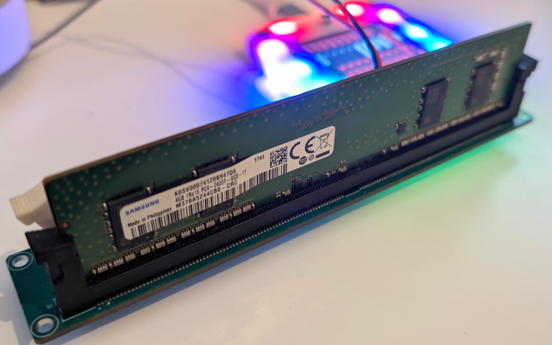
Used the generic i2c dump command to backup the DDR4 SPD to files. Noticed that i2c did not actually have save to file enabled, so I’ll push that shortly.

[0b01101100 0b0 0b0]
i2c dump -a 0x50 -w 1 -r 0x00 -b 256
[0b01101110 0b0 0b0]
i2c dump -a 0x50 -w 1 -r 0x00 -b 256

Command to dump to hex viewer.

DDR4.zip (497 Bytes)

Here’s the contents if you’d like to have a look, perhaps with this editor GUI for ddr4.

Now that we have a backup, let’s do the fun bits with the 9 volt programming voltage (lock and unlock block protection).

2 Likes
I2C> [0b01101011 0b0 0b0]

I2C START
TX: 0b01101011 ACK 0b00000000 NACK 0b00000000 NACK

Check the protected status of block 2. ACK = not protected.

I2C> [ 0b01101010 0b 0b ]

I2C START
TX: 0b01101010 NACK 0b00000000 NACK 0b00000000 NACK
I2C STOP

Try to enable protection on block two, without 9 volts on SA0. NACK = unsuccessful.

I2C> [ 0b01101010 0b 0b ]

I2C START
TX: 0b01101010 ACK 0b00000000 ACK 0b00000000 ACK
I2C STOP

Enable 9 volts on SA0 pin, then try to protect the block again. No blue smoke = success! ACK = success!

I2C> [0b01101011 0b0 0b0]

I2C START
TX: 0b01101011 NACK 0b00000000 NACK 0b00000000 NACK
I2C STOP

Check the protected status again, NACK = protected!

image

Notice some voltage droop when driving the optocoupler.

This is the current circuit for enabling 9volts.

I think this is a good change for the next revision. Enable the optocoupler via a FET instead of from the Bus Pirate pin directly.

Also add high voltage feedback to Bus Pirate with zener protection diode so we can check that 9V HV programming supply.


I gained a lot of my understanding from this project, which has a SA1 control circuit. This may be needed for older DDR, but it seems useless on the DDR4 board. I’m going to remove SA1 control.

1 Like

I also think a hole in the board right here might be nice. Big enough for a zip-tie to hold the 9volt power cable to the board so it doesn’t get lost in the parts bin.

2 Likes

From social media: Small addition of a pull-down resistor on the FET (Q1) to keep it from floating when not connected.

2 Likes

I had to do that on my blank plank glitcher. The gate on the FET floated when I disconnected the plank momentarily and burned out the small FET shorting the target to ground. Oops.

Edited: gate, not base. It’s a FET, not a BJT :blush:

1 Like

ddr4 dump command up and running.

The proper thing to do is build a ddr framework to reuse for every version, but at this stage I’m just enjoying writing bespoke code for each. Maybe we can do a framework later, or maybe this is good enough.

I2C> ddr4 probe
Block 0: Locked
Block 1: Locked
Block 2: Unlocked
Block 3: Unlocked

I2C>

Lock status.

ETA: Locking and unlocking blocks:

ETA: Read contents to file:

I2C> ddr4 read -f ddr4.bin
Read SPD NVM to file: ddr4.bin
Success :)
I2C>

Verify SPD against file:

I2C> ddr4 verify -f ddr4.bin
Verifying SPD NVM against file: ddr4.bin
Success :)

I2C>

Verify file CRC:

I2C> ddr4 crc -f ddr4.bin
Checking CRC for bytes 0-125, file: ddr4.bin
CRC verify
Stored CRC (bytes 126:127): 0x34 0x9E
Calculated CRC: 0x34 0x9E
CRC okay :)

I2C>

Patch correct CRC into file:

I2C> ddr4 patch -f ddr4e.bin
Checking CRC for bytes 0-125, file: ddr4e.bin
Stored CRC (bytes 126:127): 0x00 0x00
Calculated CRC: 0x34 0x9E
Patching CRC in file to: 0x34 0x9E
File patched successfully :)
Verifying patched file CRC:
CRC verify
Stored CRC (bytes 126:127): 0x34 0x9E
Calculated CRC: 0x34 0x9E
CRC okay :)

I2C>
2 Likes

Read a data sheet for a DDR1/2/3 EEPROM. Seems really similar to DDR4, I could see them becoming part of a combined DDR framework which could make implementation really fast.

The older eeprom is where manipulation of address pin 1 seems to come into play.

I’ll try to source a full set of common sockets and have boards made up for the remaining DDR versions.

I2C> ddr4 write -f ddr4.bin
Write SPD from file: ddr4.bin
CRC verify
Stored CRC (bytes 126:127): 0x34 0x9E
Calculated CRC: 0x34 0x9E
CRC okay :)
Writing page: 0, 1, 2, 3, 4, 5, 6, 7, 8, 9, 10, 11, 12, 13, 14, 15, Done!
Verify write
Verify: OK
Success :)
I2C>

Write to ddr4 SPD complete.

TODO:

  • Device demo
  • command docs
  • plank page
  • probe (show stats)
  • write from file
  • read to file
  • verify against file
  • check CRC
  • patch CRC in file
3 Likes
DDR4 SPD General Section Information:
=====================================
SPD Bytes Used: 384
SPD Bytes Total: 512
SPD Revision: 1.1
DRAM Device Type: DDR4 SDRAM
Module Type: SO-DIMM (0x3)
Nominal Voltage Support:
  1.2V: Yes
  1.35V: Yes
  1.5V: No
Thermal Sensor: Not present

DDR4 SPD Manufacturing Information:
==================================
Module Manufacturer ID: 0x9801 (Kingston)
Manufacturing Location: 0x05
Manufacturing Date: Year 18, Week 38 (2018-W38)
Module Serial Number: 0x92A02484 (2459968644)
Module Part Number: "ACR24D4S7S8MB-4"
Module Revision: 0.0
DRAM Manufacturer ID: 0x2C80 (Micron Technology)
DRAM Stepping: 0x42

Probe command decodes some of the SPD general and manufacturer info. I’m not 100% sure on the serial number as it is doesn’t match anything printed on the module label.

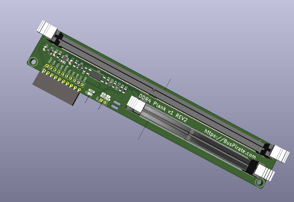
I found a $4 ewaste UDIMM, it should arrive Tuesday. After testing to make sure the UDIMM connections are correct, I’ll revise the board and order new prototypes.

Tomorrow I’ll write command docs and a device demo (using the posts here).

Pushing this to main now.

1 Like

DDR4 device demo (including screencast) is now live in the docs. Needs some editing, new photos, and tweaks when the final plank is available.

Still need to document and cast the ddr4 command, will get to that next.

UDIMM just arrived, let’s see if the plank is working.

DDR4 SPD Status:
=====================
CRC verify
Stored CRC (bytes 126:127): 0xCA 0x7F
Calculated CRC: 0xCA 0x7F
CRC okay :)

Block | Status
--------------
  0   | Locked
  1   | Locked
  2   | Unlocked
  3   | Unlocked

DDR4 SPD General Section Information:
=====================================
SPD Bytes Used: 384
SPD Bytes Total: 512
SPD Revision: 1.1
DRAM Device Type: DDR4 SDRAM
Module Type: UDIMM (0x2)
Nominal Voltage Support:
  1.2V: Yes
  1.35V: Yes
  1.5V: No
Thermal Sensor: Not present

DDR4 SPD Manufacturing Information:
==================================
Module Manufacturer ID: 0xCE80 (Samsung)
Manufacturing Location: 0x03
Manufacturing Date: Year 17, Week 41 (2017-W41)
Module Serial Number: 0xD647B920 (3595024672)
Module Part Number: "M378A5244CB0-CRC"
Module Revision: 0.0
DRAM Manufacturer ID: 0xCE80 (Samsung)
DRAM Stepping: 0x00

Excellent! UDIMM socket works. I’ll put through the final changes to plank REV1 and hopefully that’s the final update.

2 Likes

This is interesting… and messing with my very clever busy polling.

I2C> scan
I2C address search:
0x30 (0x61 R)
0x34 (0x69 R)
0x35 (0x6B R)
0x36 (0x6C W) (0x6D R)
0x37 (0x6E W)
0x50 (0xA0 W) (0xA1 R)

Found 8 addresses, 2 W/R pairs.

My idea was to make this “breadboard” friendly. 9 volt needs to be applied to SA0 pin during any lock or unlock operations. These take time, so we poll 0xa1 for ACK indicating operation is complete.

Yes, the Bus Pirate can control the 9 volts on the plank. But what if you were plankless? Then it might be handy to manually apply 9 volts or perhaps have a manual slide switch.

With that in mind, I simply polled the “new” write address during lock changes so 9 volts could be applied for the whole operation.

For example the address is 0b1010-A2-A1-A0 where Ax is the state of voltages on the address pins. Normally this is 0b1010000 (all address pins low). When A0 is at 9 volts the address changes to 0b1010001… At least it did on the SODIMM.

I2C> scan
I2C address search:
0x30 (0x60 W) (0x61 R)
0x33 (0x66 W)
0x34 (0x68 W) (0x69 R)
0x35 (0x6A W) (0x6B R)
0x36 (0x6C W) (0x6D R)
0x37 (0x6E W)

Found 10 addresses, 4 W/R pairs.

However, with the UDIMM the address doesn’t change. In fact the “normal” read write addresses disappear completely!

image

The datasheet I’m following suggests a 4ms write time. We only need to use this during lock/unlock, which are single operations, so we’re probably safe just relying on a 100ms delay between operations?

ETA: Yup! That seems to be an okay work around.

ddr4 command documentation added to the command reference.

2 Likes

That’s amazing stuff! I’ve never played with DDR, other than plugging them in to a board, haha

I did see a minor typo near the end - in the help section it states that options tell the “flash” command what to do. Looks like the kind of copy/paste thing I do all the time.

Makes me want to get the prank for no reason other than to just play with things, which is kind of the point, right? :slightly_smiling_face:

1 Like

Thank you, I pushed a fix for that and a similar error in ddr5 docs.

I was really interested in this one because while it’s a just a weird old simple EEPROM, if I looked in the Linux kernel etc to see how it works I’d be totally lost. Really fun to poke around in something that I use everyday but don’t really know a lot about.

It also seems like there is some interest in reviving DDR, and it might be useful to others. The Arduino project that inspired this little journey had dozens of pages of comments on the evga forum (before it went dark). But that still involved soldering leads onto DIMM adapters, which is probably out of reach for most PC hackers that just want to get on with it.

As of this morning we are back ordered on the DDR5 plank, and a distributor took a big chunk of the first batch. I’m hopeful we’ll save at least a few modules from the landfill.

1 Like

DDR4 ready for prototyping.

How can I get one of the DDR4 boards? I already have the DDR5 one.

1 Like