I believe it is 5V max, and it is much faster than 74hc4067 from nexperia. I will get you the data sheet. It’s a naming quirk, it is not really a CD4067 as I recall.
1 Like
Couldn’t imagine a better reason to switch to all side -emitting pixels. ![]()
Actually, if this is a concern, there are hacks that avoid a level shifter, but iirc adds another resistor. Also, it’s very possible that the pixels will accept 3v3 signals even when driven at 5v. Or a nearly identical pixel model would do so.
Or, maybe you can drive the pixel voltage at 3v3? (They are too bright anyways)
Its a bit wider range than I thought: 3-9volts:
- cd4067.zip (1.0 MB)
- SZLCSC link (if your computer can handle it…)
- I-Core site (seems to be down)
I pushed a small update:
- Remove old pull-up system
- Remove 1M pull-down
- Add footprints
- Update PCB
The good news is the PSRAM fits a treat ![]()
The whole front end needs a complete update, but we also need to find out how much less keep-out we’ll have on the next case. That should give us a bit of extra board space.
If we run the 4067 at 3.3volts, what value resistor divider should be used? Currently there are 510R protection series resistors on all pins to keep back-powering at acceptable levels. If we stick with that value we’ll waste ~10mA per pin * 12 which is basically the USB current limit.
In the past though (REV8) we had issues with the inrush to the MUX causing glitches on the IO pins. That’s why we buffer it with an op-amp. I worry if the divider uses high value resistors the delay for the MUX to settle after changing pins could get really large.
Thanks.
When you look at all the specs like resistance, propagation delay and so on, they only give them for 5V and 9V. This clearly tells me that the specs at Vcc=3.3V aren’t good and I’m a bit in doubt if using it like that is a good idea. It will probably be very temperature dependant and whatnot.
When you compare that to a Nexperia 74HC4051, they also allow Vcc up to 11V, but their recommended value starts at 2V. They also don’t give you data for 2V operation and write “When supply voltages (VCC - VEE) near 2.0 V the analog switch ON resistance becomes extremely, it is recommended to use these devices only for transmitting digital signals.” - their specs in the DS start at 4.5V, but I guess using it at 3.3V will yield much better results than the CD4067. But maybe there are even better suited analog muxes for 3.3V, I didn’t do a proper search yet.
1 Like
Ian, would having the pixels be on 3v3 be a major effort? Would avoid the need for a level shifter (for most pixels I’ve tried), and it’s rare to want them at 100% brightness (at least after novelty wears off).
Of this saves a pin or avoid need for level shifter, or if you need to level shift another signal… This is a one time engineering cost only…
1 Like
I don’t object to moving the LEDs to 3.3 in principal. We need to see if the dirt cheap LEDs we use like that. Last time we bought reels they alerted us that they switched the controller die to something cheaper, we bought old stock instead. We will have to contend with things like that as well.
Another other issue is that the LDO then has to power the LEDs and burn off that extra power as heat, so the sot89 (? From memory) LDO might need to be a bigger package to avoid heat issues.
We could do something like an SMPS, but I like to design with training wheels. I really don’t want to certify anything with switched inductors or RF. I used an LDO instead of the RP2350 on chip SMPS for similar reasons. We already spend a fortune on FCC and CE testing just messing about.
We will run an all side LEDs prototype. That’s a super minor change and we can have multiple variants assembled at once with a small discount.
I’m currently hunting quad op amps in QFN to replace the ones that are on the board. It seems like an easier target than the mux because it’s more common. Not much luck though (with cost constraints), will call around tomorrow.
1 Like
When you look at the datasheet for your cheap CD4067 it is no wonder that you had issues when switching fast: it has between 470 and 1050 ohms series resistance even when run at 5V. I can’t recommend to run it at 3.3V.
When looking at different muxes, the best would proabably be the NX3L4051. It has just 0.75 ohms max. when driven at 3.3V, specified flatness, low charge injection and whatnot. I have used it a few times and it works well. Unfortunately it is not the cheapest part. I also looked at Shanghai Belling and 3Peak, they also have very nice & cheap muxes, but unfortunately only in dual and quad configuration and not in 8:1.
The second best would probably be the Nexperia 74HCT4051 driven at 5V (Vusb), but controlled with 3.3V. It is also available in QFN. It has 100 to 180 ohms when driven at 4.5V.
Regarding the voltage divider I suggest to use a high value directly behind the GS324 opamps, something like 100k / 100k or 56k / 100k. Because you want to be able to sense near 5V/Vusb and the opamp might be rail2rail, but it will always sag a bit near the rails and this effect will get very much stronger the more current it needs to drive. But this also means you still need the LMV321 behind the mux to drive the ADC, because the RP2350 has a specced ADC impedance of 100k.
You could skimp a bit on these values and cut corners, but then your plan to use a 12bit DAC instead of saving a bit and using an 8bit one doesn’t fit to the ADC section.
1 Like
There are SMPS and SMPS.
The stuff RPi has integrated looks to me more like skittish breed, requiring a specific inductor and such. Also it must be placed directly next to the RP2350, near the ADC voltages. I guess this will not improve ADC performance.
And there are easy-going SMPS. One I have good experience with that could fit the BP is the Silergy SY8088I. Pair it with a bit more input capacitance than the minimum value from the ds, like 2x or 3x 22µF to also take the reduced capacitance of MLCCs at 5V into account, don’t do a sloppy layout and you won’t have any issues with the EMI test.
I have done this several times and had no issues. The issues I had at the EMI test lab always were with full PCBs we bought where the designers thought it would be clever to save BOM costs on capacitors for their SMPS…
Also don’t use a modern (<10 years) part from TI or Analog unless you need it for a specific feature. They try to be too clever now, and making their parts too complicated by doing so.
Would have to look at notes, but we were doing a nexperia 74hct4067 in many early revs. It was 8 or 9 rmb and hard to source at the time. The sourcing was the real issue as I recall, and that may have changed. The glitch was still there, it’s those 330 series resistors plus a weak 10k pullup in open drain modes.
I’ll take a step back and unwind all the hacks upon hacks we did to actually get it in production during the supply chain crisis. There’s 3/4 layers of hack in the amux. Cd4067->245 for 5v io ->op amps for the inrush → resistor and diodes to prevent back powering of op amps and other parts.
That’s a lot of kit, and maybe at this point a $2 ADI part is actually a better value.
Do you have one specific part in mind? Or do you mean a whole ADC with integrated 12x mux?
Like 3x of ADS1115 could work and be of course far more precise than the ADC of the RP2350, but slower. You wouldn’t neither need opamps nor voltage-dividers nor muxes. Also you’d free a bunch of pins because it is connected via I2C.
I was thinking an expensive import mux. They’re out there and small, but there’s no local production so we’re kind of stuck with what we choose.
But don’t discount the idea of using just one ADC with enough integrated channels. While the ADS1115 would be nice because it is I2C and would thus save pins, there are also other solutions, also from Chinese manufacturers. For example you could take a look at the 3Peak TPC5120. It is SPI and would need a basic voltage reference like TL431, but with 16 channels and direct sensing up to 5V and QFN case you’d get everything in one 5x5mm IC - no mux, no opamp, no levelshifter, no voltage dividers.
1 Like
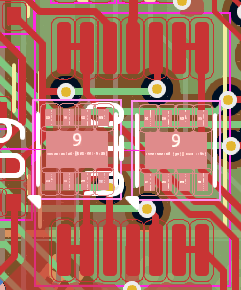
Gainsil makes a DFN 358 op-amp. Much less board space, with the disadvantage of not being able to route under it.
This week unexpected became all about the new enclosure. While waiting for the next step I’m reading datasheets.
I’m keen on the idea of farming out the ADC. The current setup served it’s purpose well, but I see a lot of potential to drastically simplify layout.
Looking at the ADS1115, it would be great to have only 4bits of measurement. It would eliminate a lot of long analog traces to the MUX.
I’m not sure how to eliminate voltage dividers, or potentially adding a level translator though.
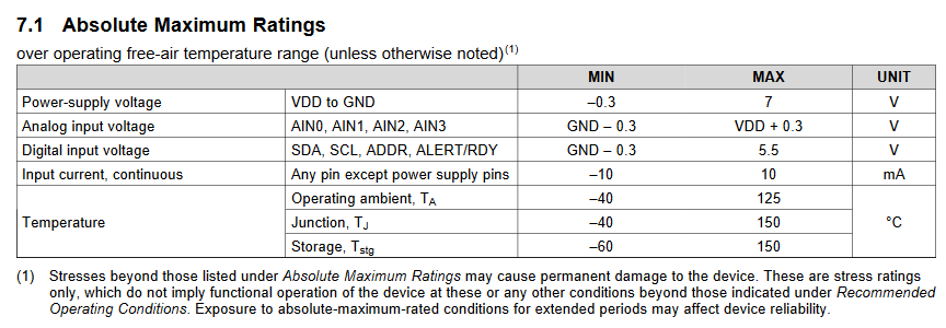
Analog inputs are +/-0.3 tolerant, so we need to keep the protection diodes and current limiting resistors to prevent back powering. That’s no biggie.
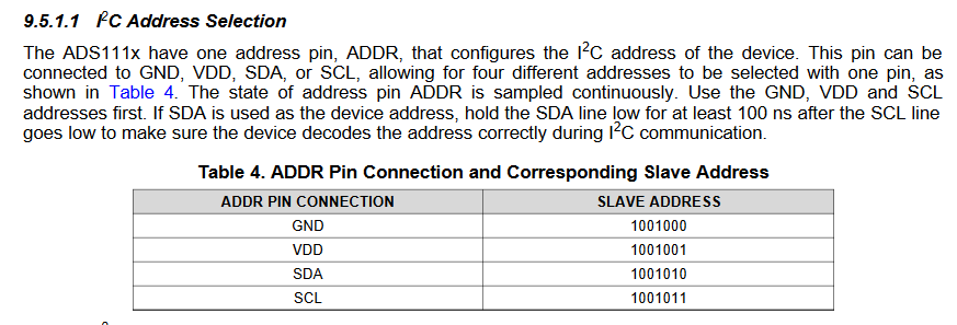
Three easy to use addresses (one not so easy). That’s perfect.
In one scenario the I2C bus will need to be run at 5volts. The RP2350 lacks 5volt tolerant inputs so we’d need a level shifter I guess?
In the other, the 1115 runs at 3.3volts, in which case we need the opamps and divide after them?
Two other considerations:
- The ADS1115 is 12.5RMB in 100s, so that’s an extra 6 USD per board (versus ~1.50 USD for the existing parts)
- We’d lose the scope mode, which is a nice educational toy. Maybe a fast SPI ADC?
I do think this is the right direction though. Maybe a combo?
8 IO pin ADC:
- Replace with 8bit SPI ADC (500khz minimum). Big change option
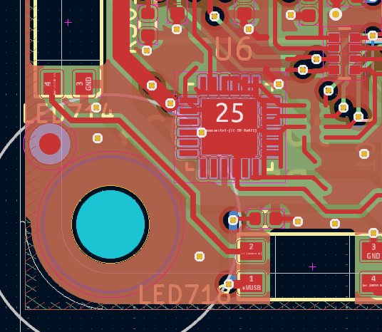
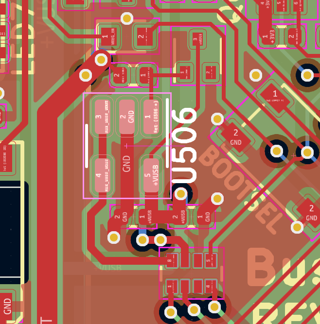
- Change MUX to HCT4059 (in QFN?). This may be cost neutral by removing the DFN level shifter which is $. Now we have room to move the output opamp down by the MUX which makes for much nicer routing.
In the image above I swapped the TSSOP14 quad opamp with 2xdual opamps in 2x2DFN. The cost increase is only 0.15RMB (0.01USD ish). It saves space and we can move those problematic resistor arrays away from the hand solder assembly area.
Other 4 signal ADC:
- The other 4 signals are VREF_VOUT, VREG_OUT, VUSB, and CURRENT_DETECT (also connected to a RP pin). Potentially also current sense (a 3.3volt scale analog voltage).
- Replace the SOT-23 opamp with a dual DFN opamp. Buffer VREG_OUT for extra protection against back powering.
- Use a 4 channel I2C ADC here to measure the internal “slow” voltages. This avoids dragging those 3 analog signals all the way to the center of the PCB.
It feels like a solution is coming into focus.
Replacing the CD4067 TSSOP24 with a 74HCT4067 in DHVQFN24 would be the easiest route to a prototype. Need to check availability on that. It is a Nexperia part, and Nexperia is now a Chinese company, so usually available somewhere.
You want to add TVS diodes to the inputs, right? Even the most low-cap optimized TVS diode for 5V will keep the voltage below 10V. Since the inputs tolerate 10mA, you just need minimum 1k series resistors as protection. No extra diodes necessary.
You could increase the series resistors and add small capacitors to create low pass filters. For example 10k and 1nF. The inputs of the ADC are high-impedance enough to not care about this. But you shouldn’t overdo the capacitance to not interfere with fast digital signals on the port.
Yes, you’d run the ADCs at 5V and add I2C level shifters. But I2C level shifting in these voltage regions is totally easy and just needs two N FETs, like BSS138W (or one 2N7002DW), search AN97055 for how to do this.
Ouch. Did you see ADS1115IDGSR Texas Instruments | Data Acquisition - LCSC Electronics - there they are 0.68 US$ @ 100pcs. which looks reasonable to me.
Did you check price and availibility of the 3Peak TPC5120? It is 1 MSPS and SPI.
Thank you for the extra info, it makes sense about the TVS diodes.
I read through the 3peak data sheet and got the basic gist of it (spi etc) and made notes about anticipated firmware challenges. I totally agree external ADC is the way to go, it simplifies the board a ton.
I put in a list of quote requests too late for today, but will get them first thing tomorrow.
Wow, you’re right, 4.33RMB. It doesn’t make sense that it would be cheaper on the international site. Wonder what I was looking at previously…
| MUX | Cost | Level shifter | Total |
|---|---|---|---|
| CD4067 (TSSOP) | 0.87rmb | 3rmb | 3.87rmb |
| 74HC4067BQ (DFN) | 5rmb | 3rmb | 8rmb |
| 74HCT4067 (TSSOP) | 6rmb | ---- | 6rmb |
| 74HCT4067BQ (DFN) | -----N/A----- | ----N/A---- |
These are quotes from the scalper (generally cheaper than SZLCSC) for variations of the current buffer setup. The HCT part in leadless wasn’t available from any of our suppliers, at least in less than a full reel.
Our favorite CAD guy is really busy and it takes a long time to get in his queue. I’m going to try to get him started on the general cleanup of the front end and placing the new I2C bus and components. Then we can have a REV0 prototype made to test the simpler changes.