If disabling is not a separate command, and uses the disable keyword with either pullup / pulldown, then you have the wierd question of what happens in the following sequence:
the second command’s text implies that it disables a pulldown. Since it’s currently not being pulled down, the interpretation has multiple options: It might do nothing, or it might disable a pullup, which is … weird.
The third command’s text implies that it sets the pulldown to zero. Since it’s not currently being pulled down, the interpretation has multiple options: It might do nothing, or it might disable a pullup, which is … weird.
Thus, I propose it is better to have the second parameter to pin essentially be a mode in which to set the pin(s). No confusion.
No, I haven’t had a chance to investigate the SPI ADC further yet. We’ll get the quote tomorrow though.
I have a few scattered thoughts on the SPI DAC. Such as, using the 4 MUX address control bits as a second SPI bus dedicated to the ADC. It would avoid a lot of the complexity of sharing one bus with LCD and NAND while maintaining similar speeds as the internal ADC.
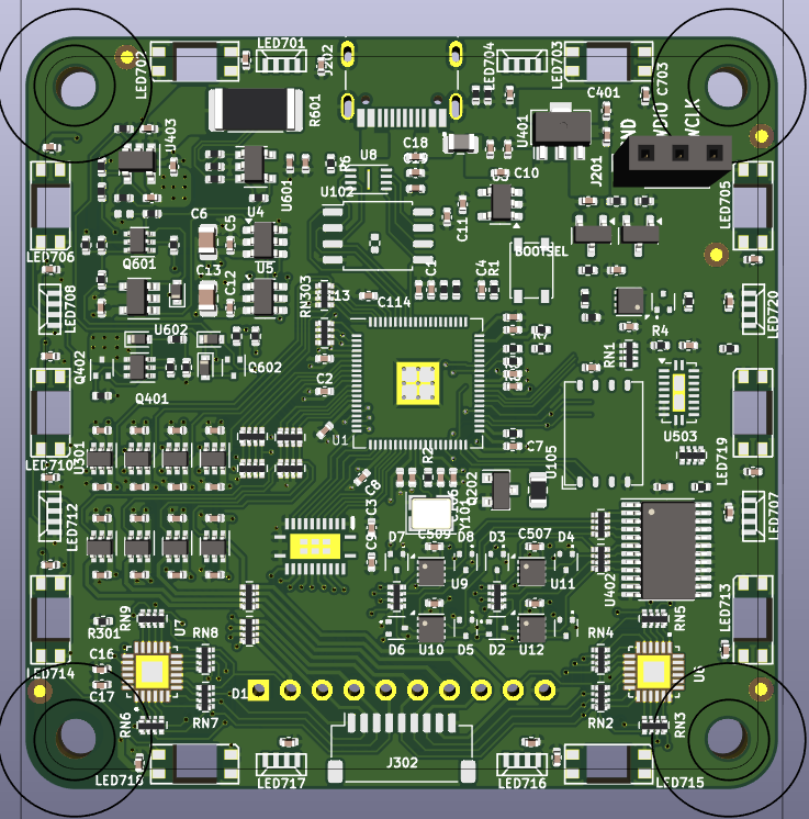
For the BP7 REV0A:
Will swap the 10uF for the switch circuit with a 4.7uf and the lower value resistor
68R ohms series resistor on the pins?
This morning we managed to find a supply of the 2Gbit NAND, so the prototypes will be populated with that
3 BOM agencies couldn’t find the 3 Peak spi ADC. Our regular guy says that 3 Peak isn’t hard to source, just this part doesn’t seem to be available. I know it’s on szlcsc, but Jin says nobody can find it.
Isn’t this just an issue during production? Or do you expect that this will pop up later in the field?
When it is just during production: wouldn’t it make more sense to do the first powerup with a proper lab power supply that has OCP configured? Especially since you don’t have much board space to spare for additional fuses. It could also affect a different cirucit in the next batch, so you’d end up with many polyfuses.
The OCP testing is is what we do at work. There the power supply is also queried by the jig control software for current draw and so on, but this isn’t really necessary if it is not part of your test plan.
You could just use the lab PSU it in a preconfigured setting for 5V and the OCP. Then wire up a special cable from the banana plugs of the lab PSU into USB-C that is plugged into the BP. When the OCP triggers the BP goes into the fail-bin.
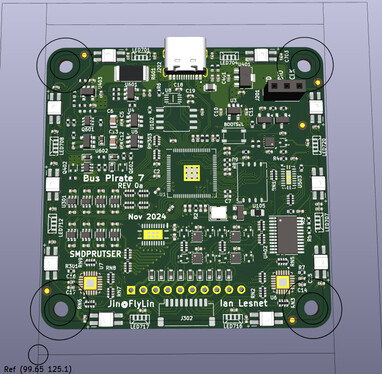
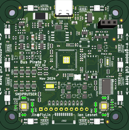
We’re gearing up production of the initial test board (7REV0). Boards will go out tomorrow, and hopefully we receive the RP2350 chips. I also need to clean up the BOM and highlight the changes and new parts to source. Then there is the issue that are reels are currently all at assembly, so we’ll be pretty slow.
REV0 is a throw-away board for testing the new I2C stuff, miniaturized analog area and PSRAM.
REV1 is in progress and includes additional power and pin protection.