I thought I’d just post a short series on a design created (but not selected) for controlling WS2812 style pixels, circa 2019, using the nRF52 series microcontroller. This post will be the TOC, linking to later posts.
1 Like
Quick nRF52840 Highlights
nRF52840 TRM / datasheet
Full datasheet / TRM v.1.8 is latest from archive.org, or get latest directly from NordicSemi.
nRF52840 ... The Good
The chip had solid support, both in Arduino
and VSCode + PlatformIO,
as well as a solid set of features:
- 64 MHz Cortex-M4 with FPU
- 1 MB Flash, 256 KB RAM
- 2.4 GHz Transceiver
- 2 Mbps, 1 Mbps, Long Range
- Bluetooth 5, Bluetooth mesh
- ANT, 802.15.4, Thread, Zigbee
- +8 dBm TX Power
- 128-bit AES CCM, ARM CryptoCell
- UART, SPI, TWI, PDM, I2S, QSPI
- PWM
- 12-bit ADC
- NFC-A
- USB 2.0
nRF52 ... The Ugly
Bluetooth support linked an opaque, closed-source blob called
SoftDevice into the firmware. This also changed various NVIC
parameters, such that the Bluetooth-related interrupts had higher
priority than anything in your own firmware, and so that supported
APIs for disabling interrupts would never disable the SoftDevice
interrupts.
As you may have noticed, the nRF52 is a single-core chip.
As a result, when the SoftDevice was enabled, and a BT packet
arrived, the SoftDevice interrupt handler would fire and
consume the processor for ~225μs (up to ~406μs).
Sending data to clockless protocol pixels (such as the WS2812)
can fail with deviations as small as 50ns. Even a 1μs interruption
is 20x that limit, so a SoftDevice interrupt that typically
took 225μs required a CPU-free method to support clockless protocols.
Example BLE Interrupt Timing and Overhead
This was pulled from the SoftDevice v1.40 specifications.
| Usage / Pattern | Max | Typ | Freq |
|---|---|---|---|
| BLE Advertising | 348,000ns | 229,000ns | 40,000ns |
| BLE Connection | 406,000ns | 219,000ns | 183,000ns |
| BLE Scanner / Initiator | 273,000ns | 175,000ns | ???,000ns |
Note: Freq is the minimum time between such interrupts occurring.
These timings only cover softdevice processing that occurs at
interrupt priority levels 0 and 1 … the CPU overhead at interrupt priority
level 4 (deferred BLE processing) can substantially increase
these values further.
Interesting nRF52 Peripherals
PPI
The nRF52 (and likely other Nordic chips) have a flexible, programmable
interconnect (PPI), which allows creating a channel from a
chosen peripheral’s EVENT. Each channel can trigger up to two
TASKs on other peripheral … and the peripherals may be distinct from each other.
The PPI runs on a 16MHz (62.5ns) clock, allowing predictable,
consistent, real-time setting of TASKs in response to any
given EVENT, from nearly any peripheral.
The configured channels can also be part of one or more
channel groups. This simplifies the simultaneous enabling
or disabling of multiple channels.
GPIOTE
There is a peripheral whose sole purpose seems to be to translate
GPIO edges into EVENTs, and support TASKs for setting, clearing,
and toggling the GPIO state.
There are of course some limitations:
GPIOTEcould not be configured on a pin used by another peripheral,
even in a read-only / snooping mode. Thus, for example, a pin
configured as part of the SPI peripheral could not also directly
generateGPIOTEevents.- Each
GPIOTEcould be configured for at most one of the following
events:RISE,FALL, orCHG(rising edge, falling edge, or
either edge).
2 Likes
WS2818 uses NRZ protocol
As you likely know, clockless pixels such as the WS2812
use a Non-Return-to-Zero (NRZ) transmission protocol,
sometimes referred to a pulse-width encoding.
In essence, the time from the rising edge to the falling
edge defines if the bit is a one or a zero. A minimum
time with no edges defines the end of data transmission,
typically orders of magnitude larger than the time to
transfer a single bit.
For WS2812:
- the GPIO idles low
- a shorter pulse is a
0bit - a longer pulse is a
1bit - total time per bit can be the same (longer low period for
0, shorter low period for1). - reset time is orders of magnitude longer (e.g., 50us (50k ns))
This is sometimes referred to in shorthand as:
T1== time from starting edge to when0bit drops lowT2== time fromT1to when1bit drops lowT3== min time fromT2to when next bit starts
For example, with T1/T2/T3 of 320/320/640 nanoseconds,
transmission of a 0 bit would be a pulse that is high
for 320ns, and then low for at least 960ns, while a
transmission of a 1 bit would be a pulse that is high
for 640ns, and then low for at least 640ns.
1 Like
An over-engineered solution. This solution was not selected, but is interesting in its combination of PPI, GPIOTE, and SPIS peripherals.
Conceptually, the solution is only somewhat complex
Everything is synchronized to the 16MHz clock from GPIOTE.
PPIchannels cause TASKs to occur in response to EVENTs.GPIOTEperipherals configured for an input pin generate
events on changes in the value.GPIOTEperipherals configured for an output pin allow
events to change the output pin state.SPISperipheral is used to serialize the data stream to a GPIO, in order to enable/disable groups ofPPIchannels.
A COUNTER peripheral is for two things:
- detect when the last data bit has been transmitted (
LAST_BIT) - detect when the required post-data delay has finished (
END_OF_DELAY)
An interrupt on LAST_BIT can be used to reclaim the data buffer, allowing preparation of the next transfer at the earliest possible time.
Slightly more detail
The SPIS peripheral reacts to the /CS line falling by loading
the first bit of output to the configured MISO GPIO. It reacts to the CLK line falling by loading the next bit of the data to transmit.
A TIMER peripheral is used to generate events:
T1→ (only when current data bit is0): sets output lowT1+T2→ ensures output low, and increments counterT1+T2+T3→ ,SCLKrise, andSCLKfall.SCLK1→ sets GPIOs for SPIS clock and for data output highSCLK0→ sets GPIO for SPIS clock low
The interesting chain is the response to the SCLK0 event:
- PPI links
SCLK0toGPIOTE(SPIS CLK).SetLow - SPIS peripheral sets MISO to next data bit
- PPI links
GPIOTE(MISO).Risingto Disable of PPI channel group ‘x’ - PPI links
GPIOTE(MISO).Fallingto Enable of PPI channel groupx
Channel group x is a single PPI, which responds to the T1 timer event, and sets the output bit low for the shorter pulse output. Since T1+T2 event always ensures the bit is low, ensuring this one event corresponds to the next data bit pushed from SPIS ensures the pulse length on the data output also corresponds to that SPIS-pushed next data bit.
Externally bridged connections
Of course, the above hand-waves a necessary evil: To control peripheral’s input GPIO (e.g., SPIS’s SCLK), a second GPIO is externally bridged. A GPIOTE task can then set / clear / toggle that second GPIO.
Similarly, to respond to changes peripheral’s output GPIO(e.g., SPIS’s MISO), a second GPIO is externally bridged. The GPIOTE peripheral can then cause events based on the peripheral’s changes to its output pin.
Full details are in later post(s).
1 Like
Continuing the over-engineered solution…
General configuration notes
In essence, everything is gated to 16MHz / 62.5ns clock.
- The PPI system is gated to 16MHz aka 62.5ns (nRF52840 specific)
- The TIMER max clock rate is 16MHz (nRF52840 specific)
- Must use either TIMER3 or TIMER4, due to # of CMP registers (nRF52840 specific)
- To ensure synchronization, the SPIS peripheral is used,
with the clock externally bridged from a TIMER peripheral. - At the start of a transfer, two steps are manually taken:
- SPIS
/CSis manually held low for at least 1000ns (1us),
ensuring the first bit is loaded and ready on SPIS MISO. - Based on whether the first bit to transfer is a zero or one,
either PPI Channel Group X will initially be configured
as enabled or disabled, prior to starting the data transfer.
- SPIS
Peripherals Used
- SPIS is used to transmit, one bit at a time, an array of bytes of data.
- GPIOTE are used to:
- generate SPIS clock
- detect SPIS output changes, and enable/disable a channel group
CHGx - control final output timing
- TIMER, with period set to match the total transmission time for a single bit
- CMP0
D0===T1; when the output pin should fall, to output a zero bit (e.g., 250ns for WS2812); also increments counter - CMP1
D1===T1+T2, when output pin should fall, to output a one bit (e.g., 1000ns for WS2812) - CMP2
SCLK=0== when SCLK should go low - CMP3
SCLK=1== when SCLK should go high
- CMP0
- A COUNTER is used with two comparators:
- CNT1
last bitto indicate the last bit has been transmitted, which also
disablesCHGy, to prevent the output from being set high again. - CNT0
delayto indicate the post-data delay has finished, and disables
CHGzto disable ALL the PPI channels used in this process. - Interrupt for CNT1 event indicates that the data buffer can be reclaimed.
- Interrupt for CNT0 event indicates transmission is fully completed.
- CNT1
GPIO Configuration
| Pin | Name | I or O | Comment |
|---|---|---|---|
| SPIS_CLK | input | As configured in SPIS peripheral registers | |
| SPIS_MISO | output | As configured in SPIS peripheral registers | |
| SPIS_CSN | input | IFalling edge causes SPIS to prepares the first output bit | |
| GPIOTE_CLK | output | Externally bridged to SPIS_CLK, controlled via GPIOTE TASK | |
| GPIOTE_MISO_RISE | input | Externally bridged to SPIS_MISO, GPIOTE event on rising signal | |
| GPIOTE_MISO_FALL | input | Externally bridged to SPIS_MISO, GPIOTE event on rising signal | |
| GPIOTE_OUTPUT | output | Final output of WS2812 data signal |
PPI Channel and Group configuration
Channel group X CHGx is defined to allow a PPI task to enable/disable
the single channel that causes a shorter pulse; changes based on rising
and falling edge of SPIS MISO.
Channel group Y CHGy is used disable the only event that sets output
high, easily enabling the mandatory idle time at the end of the data.
Channel group Z CHGz is defined to simplify enabling all the events
at the start, and disabling all the events after the final bit is transferred.
| CHG | PPI | EVENT | TASK | Comment |
|---|---|---|---|---|
.yz |
1 | CMP3(SCLK=1) | GPIOTE_OUTPUT.TASKS_SET | Sets output pin high, when CHGy enabled |
^^^^^^^^^^^^ |
GPIOTE_CLK.TASKS_SET | Sets the SPI clock high | ||
..z |
2 | CMP2(SCLK=0) | GPIOTE_CLK.TASKS_CLEAR | Set the SPI clock low (loads next data bit) |
..z |
3 | CMP1(D1) | COUNTERx.TASKS_COUNT | Increments count of total bits transmitted |
..z |
^^^^^^^^^^^^ |
GPIOTE_OUTPUT.TASKS_CLEAR | Ensures output pin set low at longer of two bit lengths | |
x.z |
4 | CMP0(D0) | GPIOTE_OUTPUT.TASKS_CLEAR | Timer sets output pin low, but only when CHGx enabled (data bit was zero) |
..z |
5 | GPIOTE_MISO_RISE | PPI.TASKS_CHG.DIS | Disables CHGx when data bit is one |
..z |
6 | GPIOTE_MISO_FALL | PPI.TASKS_CHG.EN | Enables CHGx when data bit is zero |
..z |
7 | CNT1(last bit) | PPI.TASKS_CHG[y].DIS | Disables event that sets output high |
..z |
8 | CNT0(delay) | PPI.TASKS_CHG[z].DIS | ENDS TRANSMISSION |
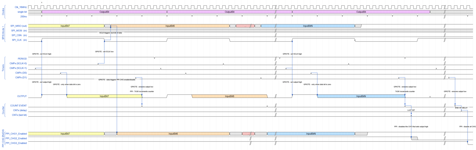
WaveDROM timing diagram
I even generated a timing diagram, to ensure there were no
edge cases / race conditions. Load the following into the
WaveDrom editor at WaveDrom Editor.
{
    "Comments" : "Load into WaveDrom editor at https://wavedrom.com/editor.html",
    "signal" : [
        { "name":"", "node":"abc" },
        ["Clocks",
            { "name": "Clk_16MHz",        "wave": "p......................................|..........................|...." },
            { "name": "single bit",       "wave": "xx8...................8................|..8.....................xx|xxxx", "data": "OutputBit OutputBit OutputBit" },
            { "name": "250ns",            "wave": "1.1...1...1...1...1...1...1...1...1...1|..1...1...1...1...1...1...|...1" },
        ],
        {},
        ["SPIS Mode 1",
            { "name": "SPI_MISO (out)",   "wave": "3...........x4..................x9.|x5.|............x1............|....", "node": ".............I..........................................................", "data": " InputBit7  InputBit6  ... InputBitN" },
            { "name": "SPI_MOSI  (in)",   "wave": "xxxxxxxxxxxxxxxxxxxxxxxxxxxxxxxxxxxxxxx|xxxxxxxxxxxxxxxxxxxxxxxxxx|xxxx", },
            { "name": "SPI_CSN   (in)",   "wave": "0......................................|..........................|....", },
            { "name": "SPI_CLK   (in)",   "wave": "0.1.........0.........1.........0......|..1.........0.........1...|....", "node": "..B.........H.............................P.........g..................."   },
        ],
        {},
        {},
        {},
        ["Timers",
            { "name": "PERIOD",           "wave": "1...................1..................|1...................1.....|...."},
            { "name": "CMPx (SCLK=0)",    "wave": "0..........0...................0.......|...........0..............|....", "node": "...........G............................................................"   },
            { "name": "CMPx (SCLK=1)",    "wave": "00...................0.................|.0.......................0|....", "node": ".A.......................................N.............................."   },
            { "name": "CMPx (D0)",        "wave": "0....0...................0.............|.....0....................|....", "node": ".....E.......................................R.........................."   },
            { "name": "CMPx (D1)",        "wave": "0................0...................0.|...................0......|0...", "node": ".................K.........................................T.......a...."   },
        ],
        {},
        {},
        {},
        { "name": "OUTPUT",            "wave": "0.1...3...........0...1...4...........0|..1...5.............0...0.|....", "node": "..C...F...........L.......................Q...S.............U...........", "data": " InputBit7  InputBit6  InputBitN" },
        {},
        ["Counter",
            { "name": "COUNT EVENT",      "wave": "0.................0...................0|....................0.....|.0..", "node": "..................M.........................................V.......b..."   },
            { "name": "CNTx (delay)",     "wave": "0......................................|..........................|..0.", "node": ".....................................................................Y.."   },
            { "name": "CNTx (last bit)",  "wave": "0......................................|.....................0....|....", "node": ".............................................................W.........."   },
        ],
        {},
        {},
        {},
        ["PPI CHG EN/DIS",
            { "name": "PPI_CHG1_Enabled", "wave": "3...........xx4.................xx9|xx5|............xx1...........|....", "node": "..............J........................................................", "data": " InputBit7  InputBit6  ... InputBitN" },
            { "name": "PPI_CHG2_Enabled", "wave": "1..................................|...|.....................x0...|....", "node": ".............................................................X........."  },
            { "name": "PPI_CHG3_Enabled", "wave": "1..................................|...|..........................|...0", "node": "......................................................................Z"  },
        ],
        {                                                                                                               },
    ],
    "edge": [
        "A-|>B  GPIOTE - set SCLK high",
        "A-|>C  GPIOTE - set output high",

        "E-|>F  GPIOTE - only when data bit is zero",

        "G-|>H  GPIOTE - set SCLK low",
        "H-|>I  SCLK triggers next bit of data",
        "I-|>J  GPIOTE - data triggers PPI CHG enable/disable",

        "K-|>L  GPIOTE - ensures output low",
        "K-|>M  PPI - TASK increments counter",

        "N-|>P  GPIOTE - set SCLK high",
        "N-|>Q  GPIOTE - set output high",

        "R-|>S  GPIOTE - only when data bit is zero",

        "T-|>U  GPIOTE - ensures output low",
        "T-|>V  TASK increments counter",

        "V-|>W  LAST BIT",
        "W-|>X  PPI - disables the CHG that sets output high",

        "a-|>b  GPIOTE - ensures output low",
        "b-|>Y  END OF DELAY",
        "Y-|>Z  PPI - disable all CHG",

        ""
    ]
}
1 Like
For those curious, the final solution used DMA, with a RAM-inefficient encoding of the data to be transferred (48 bytes per pixel instead of 3 bytes per pixel!!!)
Sine the nRF52840 has 256k of RAM, this was a “good enough” solution, and much, much simpler … only used a single PWM peripheral to DMA the data.
FIN
1 Like
What a journey!
WS2812s are such a pain. I would absolutely have added a $1 RP2040 and used PIO ![]()
I agree whole-heartedly. This work was done circa 2019, or about two years before the RP2040 shipped, so … ![]() I’ll note that in the first post…
I’ll note that in the first post…
1 Like