Three questions on PCB design process. I presume I’m just hoping for things that don’t or shouldn’t exist, but … whatever the answer I will learn something!
Q1: Are there existing “stock” footprints that support multiple parts/footprints?
If not, I've created a schematic + PCB ...
I made the following adjustments:
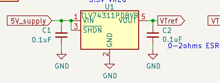
- Uses TLV75533PDRV (WSON-6, 500mA?)
- TLV74433PDBVR didn’t exist in KiCad 8.0 defaults… presumably was a 400mA version, so I went to 500mA
- J-Link Tx/Rx (COM port connection) to 3-pin header
- Can be ignored/deleted, but … may as well have the traces and drills even if not populated
- Moved LED to VTref side
- Has footprints for both through-hole and SMD for…
- Conn_02x10 (JLink 20-pin)
- Conn_01x03 (for COM port connectivity)
I wanted to stick with the built-in footprints, so I just added two components (one for through-hole, one for SMD) on those. The problem there is that the design rules checker finds tons of warnings/failures as a result of those overlapping footprints.
e.g., for Conn_02xYY_, allowing both through-hole and pass-through (creates a plated hole + the SMD solder branches)
e.g., similarly for Conn_01xYY_, having through-hole, and having both left and right SMD footprints so can use either type of part
e.g., for a given SMD capacitor / LED / resistor, a single footprint that supports multiple sizes?
e.g., for any other given part, where even though footprints vary between versions of that part, a common footprint can nonetheless be generated?
I realize that the above footprints might be targeted more towards a hacker board, not final production boards, because of the wasted space on the PCB layout. Still, these seem like useful footprints to have available, especially when wanting to maximize the ability to change parts without having make distinct PCBs.