SPI eeprom read/write/verify/erase/dump/test

Product(s) Density Max. Clock Freq. Page Size (Bytes) Write Protected
AT25010B, 25LC010A, 25AA010A 1 Kbit 10–20 MHz 8–16 Yes
AT25020B, 25LC020A, 25AA020A, 25AA02UID, 25AA02E64, 25AA02E48 2 Kbit 10–20 MHz 8–16 No/Yes
AT25040B, 25LC040A, 25AA040A 4 Kbit 10–20 MHz 8–16 No/Yes
AT25080B, 25LC080C, 25LC080D, 25AA080C, 25AA080D 8 Kbit 10–20 MHz 16–32 No/Yes
AT25160B, 25LC160C, 25LC160D, 25AA160C, 25AA160D 16 Kbit 10–20 MHz 16–32 No/Yes
25CS320, AT25320B, 25LC320A, 25AA320A 32 Kbit 10–20 MHz 32 Yes
25CS640, AT25640B, 25LC640A, 25AA640A 64 Kbit 10–20 MHz 32 Yes/No
AT25128B, 25LC128, 25AA128 128 Kbit 10–20 MHz 64 Yes
AT25256B, 25LC256, 25AA256 256 Kbit 10–20 MHz 64 Yes/No
AT25512, 25LC512, 25AA512 512 Kbit 20 MHz 128 Yes
25LC1024, 25AA1024 1 Mbit 20 MHz 256 Yes
AT25M01 1 Mbit 20 MHz 256 Yes
AT25M02 2 Mbit 5 MHz 256 Yes
25CSM04 4 Mbit 8 MHz 256 Yes

A short list of initial 25X SPI EEPROMs to investigate. Similar to I2C EEPROMs, some use the upper bits of the write enable instruction to select memory blocks out of range of the address pointer.

Product(s) Density Size (bytes) Page Size (Bytes) Address Bytes Block Select Bits
AT25010B 1 Kbit 128 8 1 0
25AA/LC010A 1 Kbit 128 16 1 0
AT25020B 2 Kbit 256 8 1 0
25AA/LC020A, 25AA02UID (32 bit ID, 0XC0 locked, location 0xFA-0xFF)), 25AA02E64/48(64 or 48 bit EUI-x Node Address, 0XC0 locked, location 0xFA-0xFF or 0xF8 to 0xFF) 2 Kbit 256 16 1 0
AT25040B 4 Kbit 512 8 1 opcode 0x02 bit 3
25AA/LC040A 4 Kbit 512 16 1 opcode 0x02 bit 3
25AA/LC080C 8 Kbit 1024 16 2 0
AT25080B, 25AA/LC080D 8 Kbit 1024 32 2 0
25LC/AA160C 16 Kbit 2048 16 2 0
AT25160B, 25LC/AA160D 16Kbit 2048 32 2 0
25CS320 (ECC), AT25320B, 25LC/AA320A 32 Kbit 4096 32 2 0
25CS640, AT25640B, 25LC/AA640A 64 Kbit 8192 32 2 0
AT25128B, 25AA/LC128 128 Kbit 16384 64 2 0
AT25256B, 25LC256, 25AA256 256 Kbit 32768 64 2 0
AT25512, 25LC512, 25AA512 512 Kbit 65536 128 2 0
AT25M01, 25LC1024, 25AA1024 1 Mbit 131072 256 3 0
AT25M02 2 Mbit 262144 256 3 0
25CSM04 4 Mbit 524288 256 3 0
2 Likes
static const struct spi_eeprom_device_t eeprom_devices[] = {
    { "25X010",    128,     1, 0, 0,   8, 10000 }, //8 and 16 byte page varients
    //{ "25X010",    128,     1, 0, 0,  16 },//use the lowest common page size
    { "25X020",    256,     1, 0, 0,   8, 10000 },
    //{ "25X020",    256,     1, 0, 0,  16 },
    { "25X040",    512,     1, 1, 3,   8, 10000 },
    //{ "25X040",    512,     1, 1, 3,  16 },
    { "25X080",   1024,     2, 0, 0,  16, 10000 },
    //{ "25X080",   1024,     2, 0, 0,  32 },
    { "25X160",   2048,     2, 0, 0,  16, 10000 },
    //{ "25X160",   2048,     2, 0, 0,  32 },
    { "25X320",    4096,     2, 0, 0,  32, 10000 },
    { "25X640",    8192,     2, 0, 0,  32, 10000 },
    { "25X128",  16384,     2, 0, 0,  64, 10000 },
    { "25X256",  32768,     2, 0, 0,  64, 10000 },
    { "25X512",   65536,     2, 0, 0, 128, 10000 },
    { "25XM01",  131072,     3, 0, 0, 256, 10000 },
    { "25XM02",  262144,     3, 0, 0, 256, 5000 }, //5MHz
    { "25XM04",  524288,     3, 0, 0, 256, 8000 } 
};

I narrowed the list of SPI EEPROMs down to this set with common page sizes and addressing methods.

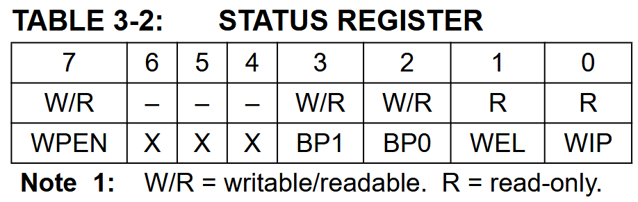
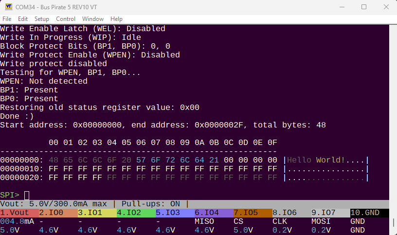
The status register bit 0 indicates a write is in progress, bit 1 indicates if the write enable latch is set (data can be written to the memory or status register).

Write protection blocks

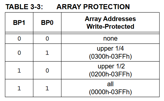
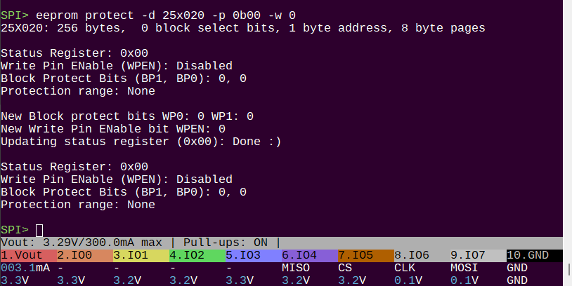
Many, but not all, EEPROMs have a write block protection feature. This allows you to protect a portion of the EEPROM from being written to, even if the write enable latch is set. The block select bits are used to select which block is protected: none (0b00), the upper 1/4 (0b01), the upper 1/2 (0b10), or the entire EEPROM (0b11).

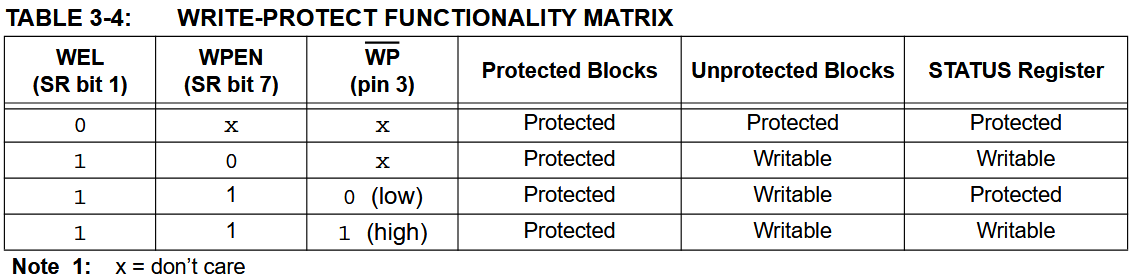
Fewer devices have a WPEN bit that disables the Write Protect (WP) pin. When WPEN is 0, the WP pin is ignored. When WPEN is 1, the WP pin is used to control write protection. If the WP pin is high, the EEPROM is write protected. If the WP pin is low, the EEPROM can be written to.

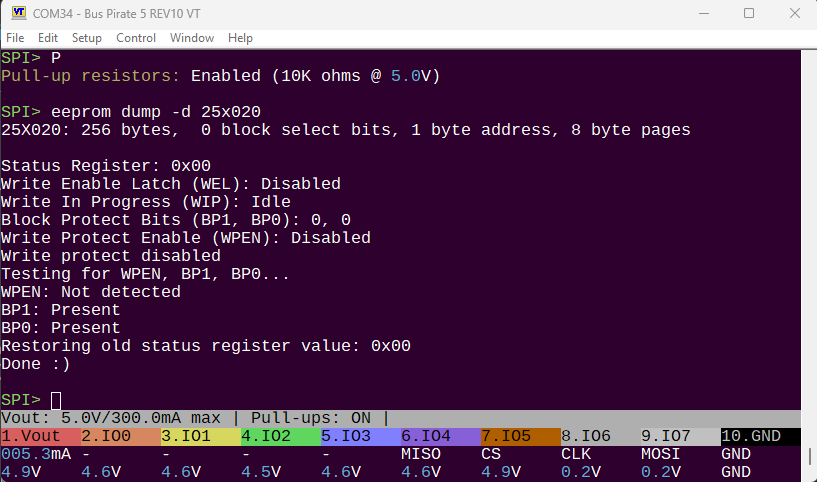
We can test which bits are available in a chip by writing 0b10001100 to the status register, enabling all the protection bits. If the chip supports WPEN or BPx bits, they will be set to 1 after the write. If they are not supported, they will remain 0. This chip has BPx bits, but not WPEN bit.

ETA: dump working, with new greyed out regions not requested by the user:

Bug?: The start address above is showing as 0x00000000, but the color coding suggests the user requested a dump of 0x1D bytes starting at offset 0x06.

Option: If the user didn’t request some of the data, consider just not printing it? Thus, it might look like:

        | 00 01 02 03 04 05 06 07 08 09 0A 0B 0C 0D 0E 0F
---------------------------------------------------------
00000000:                   57 6F 72 6C 64 21 00 00 00 00 |      World!....|
00000010: FF FF FF FF FF FF FF FF FF FF FF FF FF FF FF FF |................|
00000020: FF FF FF FF                                     |....            |

Benefit: Only printing the requested bytes ensures that, even without color information, the data requested is clearly delineated.

1 Like

In the latest iteration unrequested bytes are dark grey. My thought is that we already have the data row, and it’s handy to have context even if it’s not your first priority.

For example request a field of DDR5 SPD data, but also see the previous and next field so you know you’re in the right place. I’d appreciate that when messing with a new chip.

When this all pans out the header row will be updated (or removed?) To make clear what exactly is happening under the hood. I haven’t quite sketched that part out yet.

You’re right, the extra data is useful for context.

And I wonder … couldn’t the user just ask to dump that extra data?

Other questions I have:

  1. What defines the “extra data” count that is printed to either side of the requested data?
  2. If the “extra data” count is based on a 16-bytes per row layout, what happens when you extend the API to 8-bytes per row, or allow other bytes-per-row dumping? (e.g., useful for packed arrays of a 6-byte struct)
  3. If the “extra data” is based on the chip returning data in 16-byte blobs, what result is expected for a chip that only reads in 512-byte blobs?

Thanks!

1 Like

Currently we are only addressing 8 bit devices with 256 byte address pages.

Today i changed the ui_hex functions to take a configuration strict. It is much easier to use, and if we get to little/big endian 16 or 32 bytes we can address it through the config struct. This is prototyped on the spi_eeprom branch.

It’s so hot that my palms are sticking to the computer table, so that’s a good sign to call it a day.

Lots of progress. Refactored the code to be a “universal” programmer for multiple bus types and memory types. This was way more work than expected, and I still have to port I2C eeprom to the new framework.

SPI> eeprom protect -d 25x020
25X020: 256 bytes,  0 block select bits, 1 byte address, 8 byte pages

Status Register: 0x0C
Write Enable Latch (WEL): Disabled
Write In Progress (WIP): Idle
Block Protect Bits (BP1, BP0): 1, 1
Write Pin ENable (WPEN): Disabled

SPI>

Show the block write protect status.

SPI> eeprom protect -d 25x020 -t
25X020: 256 bytes,  0 block select bits, 1 byte address, 8 byte pages

Status Register: 0x0C
Write Enable Latch (WEL): Disabled
Write In Progress (WIP): Idle
Block Protect Bits (BP1, BP0): 1, 1
Write Pin ENable (WPEN): Disabled

Testing support for Write Protect blocks (WP0, WP1) and Write Pin ENable (WPEN)

Disabling write protect: 0x00, OK

Testing for BP0, BP1, WPEN...wrote: 0x8C, read: 0x0C
BP0: Present
BP1: Present
WPEN: Not detected

Restoring original status register: 0x0C...Done :)
Status Register: 0x0C
Write Enable Latch (WEL): Disabled
Write In Progress (WIP): Idle
Block Protect Bits (BP1, BP0): 1, 1
Write Pin ENable (WPEN): Disabled

SPI>

Test if block protect and WPEN are supported. This chip has block protect, but not WPEN.

SPI> eeprom protect -d 25x020 -p 0b00
25X020: 256 bytes,  0 block select bits, 1 byte address, 8 byte pages

Status Register: 0x0C
Write Enable Latch (WEL): Disabled
Write In Progress (WIP): Idle
Block Protect Bits (BP1, BP0): 1, 1
Write Pin ENable (WPEN): Disabled

Writing status register block protect bits, WP0: 0 WP1: 0...Done :)
Status Register: 0x00
Write Enable Latch (WEL): Disabled
Write In Progress (WIP): Idle
Block Protect Bits (BP1, BP0): 0, 0
Write Pin ENable (WPEN): Disabled

SPI>

Update the block protect bits

TODO:

  • Make BPn bit display consistently
  • Lacking ability to update WPEN
  • Port I2C eeprom command to new framework
  • 1-Wire eeprom support
  • Update everything to the new ui_hex_X_config functions.