SPI `flash probe` broken?

Continuing from Buspirate v5 rev 10 SPI Delay - Cannot dump chip:

Today, I built / flashed latest main (0d8d8da from last week, "Update to latest version of minmea gps decoder).

I then attached the WSON8 plank (REV3), filling the 6x8 slot with a chip that I really want to get a dump of. Unfortunately, I wasn’t getting any response from the chip. I remember having this type of problem before, so I search the archives and found the above thread. So I manually set BPIO 0..3 to HLHH, following that thread’s learnings.


BusPirate terminal commands

HiZ> m spi

Mode: SPI

Use previous settings?
 SPI speed: 10 kHz
 Data bits: 8
 Clock polarity: Idle LOW
 Clock phase: LEADING edge
 Chip select: Active LOW (/CS)

y/n, x to exit (Y) > y

SPI> A 1
IO1 set to OUTPUT: 1

SPI> A 0
IO0 set to OUTPUT: 1

SPI> a 1
IO1 set to OUTPUT: 0

SPI> A 2
IO2 set to OUTPUT: 1

SPI> A 3
IO3 set to OUTPUT: 1

SPI> flash probe


Initializing SPI flash...
Flash device manufacturer ID 0x00, type ID 0x00, capacity ID 0x00
Error: SFDP signature error. It must be 0x50444653 'SFDP'
Warning: Read SFDP parameter header information failed.
Warning: The chip does not support JEDEC SFDP.
Searching flash chip database for 0x00 0x00 0x00
Error: Flash device not found
Error: device not detected

SPI> 

Unfortunately, still no signs of life.

Thinking I somehow killed the chip (e.g., overheating? if that’s even a thing?), I grabbed the WSON8 I saved from an alpha BP7 board, and put that into the adapter. Unfortunately, I got the same result.

The chip is a WINBOND W25N01GVxxxG/T/R (datasheet). Nothing jumps out at me as problematic…

So I dug deeper. flash probe was reporting the following line of output:

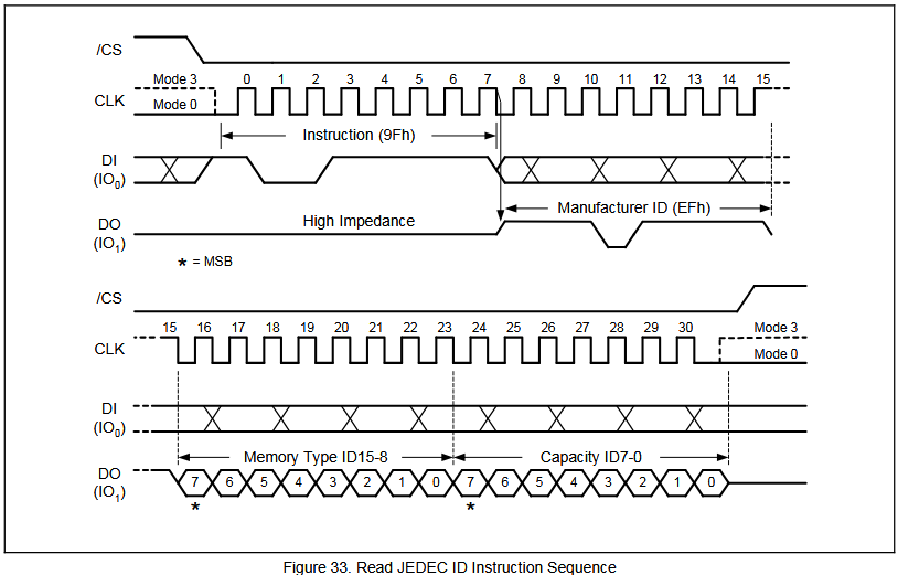
Flash device manufacturer ID 0x00, type ID 0xEF, capacity ID 0xAA

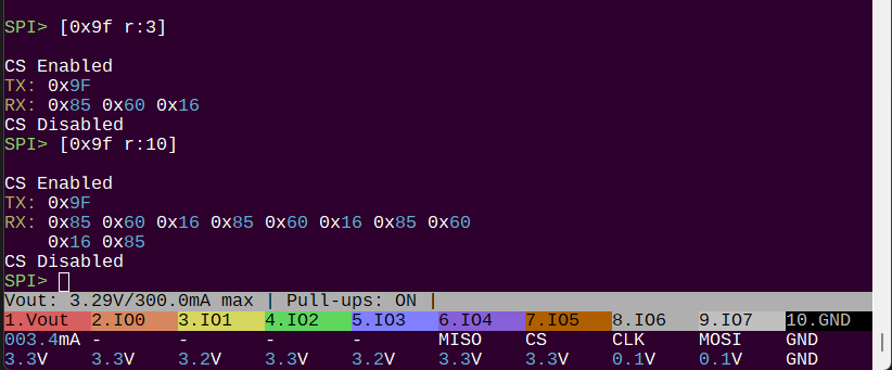
However, using bus syntax, manually requesting the JEDEC ID worked fine:

SPI> [ 0xFF ] D:100 [ 0x9F r:4 ]
...
TX: 0x9F
RX: 0x00 0xEF 0xAA 0x21

Is the flash probe command broken, where it fails to skip over the first dummy byte (here, 0x00)? Obviously, if it’s reading at the wrong byte offset, it won’t properly identify the chip.

Both the recovered BP7 and new WSON8 chips seemed to work properly using bus syntax, and failed the same way using flash probe.

I would welcome any thoughts. Also, I may be slow to respond until Monday…

2 Likes

I’m not having any issues with the latest firmware.

Question: are you trying to power through IO0 and IO1? The purpose behind the switches and redundant connection is to access chips with a different pinout, rather than power the chip through the IO pins.

  1. Ensure that the slide switches are towards the body of the Bus Pirate (VOUT/GND position).
  2. I would increase speed to 100kHz minimum.
  3. Instead of setting the A/a pins, just use P to enable pullups, it has the same effect on WP and HOLD.
  4. This is a big one that stands out: in the example I don’t see a power supply being enabled (W 3.3)
2 Likes

I got commands between the chip and buspirate working. What I’ll look at (likely Monday) is the bug(?) in probe where it does not send the dummy byte following the command, and then interprets the (0x00) dummy data as the first byte of the response.

I have to check if the dummy byte is unique to W25N winbond chips, but I don’t believe so…

I also validated some data by manually reading from the chip. Something is awry, but what is TBD (chip having different requirements? wetware? other?)

I can’t look for a couple days, but it was helpful to know that you are not having any issues.

1 Like

ID should be standard.

But what about the power supply? Sometimes a chip can be back powered through other pins and will give a little response but when you really query it just doesn’t have the juice to reply.

If ID is standard, then there is a bug. Dataset for this chip shows after sending the command byte to get the JEDEC id, there is a dummy byte (eight clock cycles where neither side generates data).

flash probe is not sending the dummy byte, and so must ignore the first byte when reading. It must do one of those two things, right?

On road, so limited access for me to datasets right now….

The datasheet you link does show a dummy byte before the JEDEC ID. I have never seen one like that before.

There are two different libraries the flash command uses to probe flash. I wrote a probe library and we incorporate the Serial Flash Universal Driver Library project. While it’s always possible my code is messed up, the SFUD is pretty widely used and well developed.

Here is the 9f command from the common W25QXXX flash that is on the Bus Pirate and also included with the flash adapter boards. This is pretty typical to me, with no dummy byte required.

It’s possible the W25Nxxx chips are not directly compatible with the W25Q. I’ve never heard of the N version, only the Q type.

1 Like

How can anyone NOT love a standard where the most basic identification command is incompatible across versions?

Looks like I’ll have to figure out if this is reported in the capabilities page somewhere, presuming of course that isn’t similarly incompatible.

Or maybe have to heuristically determine this when first byte is zero but otherwise real data is returned.

2 Likes

JEDEC Manufacturer IDs Are a Mess. The whole thing wasn’t exactly thought out well :slight_smile:

Had some time to look over the datasheet. Also found the W25M02GV, which seems to be the same but with 2 x 1Gbit dies stacked in the same package.

The W25N01GV is NAND memory, like the chip that stores the Bus Pirate file system. The flash command is targeted at serial NOR memory. I’m not sure how similar the read/write process is.

Also noted that the W25N01GV doesn’t support 0x5A serial flash parameter table command, so that’s why SFUD can’t get a lock on it.

I’m really curious about this chip, and wonder if it isn’t a welcome alternate part for the Micron NAND chips we currently use.

I’m just trying to figure out a reliable way to get the JEDEC ID:

Current thoughts are, after sending the command byte, is to read the bytes from the device one at a time. Maybe something such as:

int delayCount = 0;
int bank = 0;
byte firstByte = 0x00;
do {
    // read the next byte as a ***potential*** device response
    firstByte = ...
    // note: data should be 0x00, but maybe someone used pullups
    // instead of pulldowns.  Simple to check...
    if ((firstByte == 0x00) || (firstByte == 0xFF)) {
        if (bank == 0x00) {
            ++delayCount;
            continue; // next loop iteration
        }
        else {
            /* error ... likely not a device response*/
            break;
        }
    }
    else if (firstByte == 0x7F) {
        ++bank; // continuation banks, oh my!
        continue; // next loop iteration
    }
    else {
        // got the first byte of the JEDEC (or garbage ... hard to know)
        // either way, only read two more bytes
        break
    }
} while (true); 
// Then read the next two bytes from the device
1 Like

I’m not sure the JEDEC ID command is reliable enough to determine if the chip is this NAND or a NOR. I suppose you could just read four bytes and compare to a known list. I don’t think I’ve seen a NOR flash give a bank continuation byte before, but I haven’t verified that.

image
image

There are other incompatibilities as well. NAND has a dummy byte on the read.

image
image

Also block erase.

I didn’t dig in too deep, but it also looks like there is some funky addressing when EEC is involved.

It looks like the flash command is currently setup for maximum 256 byte page size, and I believe the NAND page size is 2048/2112 (without EEC) bytes.

Allow me to address each of those:

JEDEC ID

Reading only four bytes is not enough to retrieve a JEDEC ID from an unknown chip for at least two reasons:

  1. Variable delay requirements (aka dummy bytes).
  2. Variable manufacturer “bank”. That’s right, they didn’t have enough space for all the manufacturers, so if the first data byte is 0x7F, you increment the “bank” in which you lookup the manufacturer, and skip to the next byte.

This can be safely read, it just takes a bit of finesse.

  1. Presume you can read one byte at a time, and stop anytime.
  2. Read / skip until you get non-0x00 and non-0xFF (treat as delay / dummy bytes).
  3. Read / skip until you get non-0x7F bytes (treat these as bank increments).
  4. Read the three bytes as per “typical” chips

Delays in other commands

Yes! This is why it’s critical to have a solid way to read JEDEC ID.

Eventually, the delay count determined from reading the JEDEC ID might be usable directly for the other commands. However, for the shorter term, it will likely be per-command settable for the commands used in the firmware for read / write / dump, and determined by the extracted JEDEC ID ({ bank + manu + two bytes }).

Addressing

Can you help me understand what you saw that was odd in the addressing?

1 Like

I’ve only seen banks used on JTAG interfaces. NOR flash uses a single byte ID in every chip I’ve used, and newer stuff like the DDR5 SPD hub uses two bytes: bank and ID.

This is the result of 0x9f on a PUYA NOR flash. PUYA is definitely not bank one material :smiley: Also note that reading beyond the 3 byte boundary rolls over and repeats the JEDEC ID.

I would also caution that the “type and capacity” ID fields are not standard and largely meaningless. Each manufacturer decides how to use it. Some have a proper capacity encode system, some just have model number type encodings. I am 99% sure I’ve seen overlap in the JEDEC IDs for different chips from the same manufacturer.

My understanding is the NOR flash JEDEC ID is basically a way for firmware developers to determine what chip is installed of a known set. For example small and large capacity version of the same product, or when the chip used in production changes for some reason.

1 Like