I’m trying. to test the SPI code and I am not having much luck. I am using the pinout on the display.
IO7< =>CDO < = > D0
IO6< = > SCLK < = >CLK
IO5 < = > CS < = > SS
IO4 < = > CDI < = > DI
GND < = > GND
Vout < = > Vcc
Do you have a breakout board with components, or just a chip in a board?
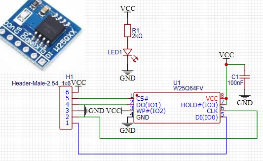
I’m working with this chip now. The WP and HOLD pins need to be high, the aliexpress breakouts have resistors to do this. I use an adafruit SO8 adapter board and I use Io0 and io1 to pull WP and HOLD high
The command is:
A 0; A 1
To put IO0 and IO1 high.
Also be sure you have power on the buffer from and external source or using the W command to enable the bus pirate power supply.
Yes. After swapping DI/DO and pulling up WP AND hold it works. So BP CD0 goes to DI on the breakout board? Like the TX/RX connectors go to the RX/TX pins.
Yes, and good reminder I should add an arrow to the display, thank you! The UART has arrows, but SPI usually uses the now politically incorrect MOSI MISO notation. Thought, flash chips mostly do Di and DO and you experienced.
I’m working on exactly those adapters. Happy to send you one when I get the PCBs.
Would it make sense to have a special mode for flashrom where the display mentions the connection of the WP and HOLD pins, and then perhaps checks to see if they are correct, and warns if they are not? I’m thinking bare breakout boards, board with pull-ups, and fully populated PCB’s - powered and unpowered. (I’m not sure how successful it would be dumping flash on populated boards.
I’m really stuck on that one. Designing the wall between a mode and a command is still forming as I work through the firmware. My roadmap is 1. Get flash working with majority of chips from terminal 2. Do BBIO gpio and spi bin access modes, get flashrom or others working. 3. Use the opportunity to refactor the former to deal with 1. And 2. Better.
