2Gbit / 4Gbit SPI NAND flash (upgrade) chips

ImportedPhoto_1708958362901

I really don’t recommend you do this, but in theory it should be possible to double or quadruple the flash storage. I added the 2Gbit and 4Gbit SPI NAND flash chips to the Dirty PCBs shop if anyone wants to mess with it.

Bus Pirate 5 is mounted with a 1Gbit MT29F1G01ABAGDWB-IT:G NAND flash chip that formats to approximately 100 megabytes. The page size is 2K, it has a single plane of flash.

MT29F2G01ABAFDWB has 2Gbit of NAND flash. The page size is also 2K, but it has two planes to select from. Upgrading to this flash chip would probably involve changing the end address/number of pages in the nand.h flash setup files and figuring out how to switch planes. Planes could be swapped on the fly, or used as two separate partitions. I have not looked that closely.

MT29F4G01ABAFDWB is the 4Gbit NAND version. The page size is 4K, but it only has a single plane. Upgrading to this flash chip could involve expanding the read/write buffer in the nand.c/h functions and updating the end address.

Swap chips at your own risk. There’s no software or firmware support (planned) for these chips, but the Bus Pirate is a hacker tool and things happen.

The 2Gbit is actually cheaper than the 1Gbit used on BP5. The 4Gbit is hard to source and much more expensive. You may be able to find one of them locally at a lower cost.

There are some trade offs because of how the chips are split into “planes” and the page size. This could be a really easy upgrade in the lower level NAND functions, or it could involve digging into the guts of dhara, our NAND flash management library.

2 Likes

I have an engineer willing to support the 2gb version. See my dm for more info. @ian @Bus-Pirate

Thanks! Replied.

It looks like we are going to send a handful of Bus Pirates back to the assembler to have the 2gbit chip attached. I’ll send some to @BusPirateV5 , and put a few in the store.

If you’re thinking about getting a 2Gbit NAND board: Please remember there is absolutely no support for the 2Gbit chip at the moment, and it may not even be feasible to work with the second plane. I mounted the chip on an old development board and it does not work out of the box. I can get the chip ID and such, but it will take some messing about to get the plane swap working.

1 Like

Thank you @ian. I’m excited to see can be pulled together and am happy to support him in his efforts.

The other engineer us intending to dig into the dual plane 2gb nand and see if he can get it functioning on the second plane as well. I have hope, but will keep the thread updated if he doesn’t join the forum conversation himself for any reason.

1 Like

Sorry for the delay, the 2Gbit version is available here.

It’s $1 more expensive than the normal Bus Pirate 5, hopefully that will discourage accidental buys. As always: if you buy a developer board and contribute some code, we’re happy to refund the cost of the hardware. We’d give it away for free, but there’s no sustainable way to handle that in an online shop :slight_smile: You can also write me for a free board if you’re interested in working on the new features.

2 Likes

1 order delivered. Excited to hear initial thoughts.

2 Likes


2GB nand board #2 has arrived!

There is no promise it’s even feasible, but i will provide updates when available.

2 Likes

No worries if nobody gets it going. It’s nice to be able to send bespoke hardware on demand :slight_smile:

1 Like

It is greatly appreciated! You are really killing it!

Do you have the datasheet for the MT29F2G01ABAFDWB chip?

I want to understand the “two plane” aspect, but cannot seem to find the datasheet for this particular chip.

Also, can you help me understand why the end address and page size are hard-coded, rather than asking the chip to report via READ PARAMETER PAGE (ECh)?

Yes, it is a pain to find. Farnell is the only place I found it. I have signed up/been redirected by microns site so much I got dizzy :roll_eyes:

The underlying bad block management/wear leveling library is Dhara. In the Bus Pirate firmware this is in the /dhara/ folder.

Integration with the micron nand is based on this example. The chip details are hardcoded here and the device ID here, but indeed the chip is able to identify itself. In the Bus Pirate firmware this is in the /nand/ and /fatfs/ folders.

This is speculative, and I don’t want to “jinx” it… In the limited poking about I’ve done, I do not think it is a very difficult update. Something like:

  • Add additional chip details or query the chip for details during initialization
  • The 2Gbit chip is divided into 2 1Gbit planes. I’ve not dug in here, but “something” has to be added to swap between the planes.

The 4Gbit chip is rare and expensive. It has a single plane, but it has 4K sectors that we have to load into RAM. Which I take to also mean we’ll thrash the chip more because files (scripts, config files) are mostly pretty small.

2 Likes

I’ll dig in and learn some, thanks for the pointers!

And you’re right … this is because the FAT file system was not designed to be used directly on this type of media. exFAT can do much better with this media, with some minor tweaks, because it allows a file to pre-allocate a larger chunk of the media than it actually needs. I don’t think that capability was in FAT32 (or earlier). Pretty much every OS I’m aware of now has exFAT support, so that might be the first change I consider testing.

I’m still worried that the current implementation, where the FS is surprise-removed from the host, will cause problems, and am thinking through alternative designs for your consideration…

1 Like

Follow up to add: there are SD card chips (I assume an SD card die bonded in a chip) that integrate the wear leveling and such. I have two issues with these chips:

  1. SPI speed is low (according to datasheet, around 20mhz max), so we have to run the LCD slower as well or they become misconfigured (in my experience)
  2. They use the standard SD card command set, which the SD Card association claims a patent over. I can’t believe the patent is not (close to) expired, but they still have a plastic sign in the window and want 2K (5K?) a year to sleep well at night. I don’t personally want to have annually licensed stuff in my open source projects, even if the fee is relatively low. I contacted the EFF.org to see if they would post some open advise on using SD cards and SD card compatible tech in open source, but they weren’t interested.

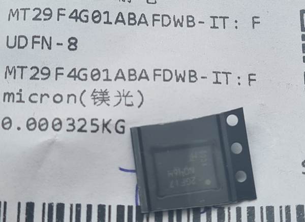
This is just some notes as I try to parse this model. Maybe you (or others) will find some of it useful. Initially, this is focused on the simplest use model (single block read / write).

NOTE: I have NOT gone through the source code yet … this is strictly a mental model of how to access/use a multi-plane SPI NAND chip.

Memory Layout

See, generally, Figure 7 on page 11.

  • Cache Register - most recently read block from NAND
  • Data Register - used to write to the NAND (+)
  • Cache Register and Data Register sizes are one block (each)
  • Each plane has its own Cache Register and Data Register

Sequential blocks are on alternating planes. (Even blocks on one plane, Odd blocks on the other.) For two-planes such as this chip, the plane corresponds to the least significant bit of the block address. For four-plane chips, the two least significant bits of the block would indicate the plane.

Reading Data from NAND

Generally, reading the data from the NAND is a multi-step process. A PAGE READ command reads data from a given block address into the corresponding plane’s Cache Register. Completion status must be checked via the GET FEATURES command. No changes needed to support multi-plane for this part.

Once the data is in the Cache Register, any amount of those bytes can be read using a READ FROM CACHE commmand. Because each plane has its own Cache Register, these commands now include an indication of which plane’s Cache Register to read from.

Writing Data to NAND

Generally, writing data to the NAND is also a multi-step process. First set of commands place data into a Cache Register via PROGRAM LOAD command. Because each plane has its own Cache Register, these commands now include an indication of which plane’s Cache Register to write to.

Once the block’s data is in the plane’s Cache Register, it is written to the NAND via a PROGRAM EXECUTE command. The block address is explicitly provided, which implicitly indicates the plane.

Single code path … problem?

The number of planes for a given device does not appear to be exposed via the Parameter Page? (See page 26 / Table 4). Theoretically, this could make it difficult to seamlessly support both single and multi-plane devices.

HOWEVER … the plane bits are simply overloading four dummy bits that were previously unused. If testing confirms that the single-plane chip ignores the four dummy bits, and that the two-plane chip ignores the three dummy bits, then support for up to 16-plane devices (2^4) can be implemented with a single, common code path as follows:

ALWAYS replace the four dummy bits with the low four bits of the block address.

  • A single-plane chip will ignore those dummy bits
  • A two-plane chip will ignore the top three bits, and use the least significant bit to select the plane
  • A four-plane chip will ignore the top two bits, and use the two least significant bits to select the plane
  • etc.

Summary

Any commands that previously implicitly acted on either a Cache Register or Data Register, and which did not already provide a target block address, must now including bit(s) to indicate which plane’s register(s) that the command is targeting.

The most obvious examples are the READ FROM CACHE command and PROGRAM LOAD commands.

Command OpCode Page Figure
READ FROM CACHE 03 or 0B 18 13
PROGRAM LOAD 02 29 20

Conclusion

This seems like it should be a fairly low-overhead change. Some testing should be done of both the single-plane and multi-plane chips, to ensure they ignore the dummy bits that are not relevant to their specific layout.


(+) and also used to allow multi-sector reads to be more performant, but that is unlikely to be used in BP5(?)

P.S. - Given the simplicity of the model used by BP5, none of the benefits of multi-plane NAND are expected (at least initially).

1 Like

Really nice summary, thank you. If they both have write cache it seems like a RAID situation would be the thing to optimize performance?

It’s not really a write cache, and there is only a single busy bit for the whole NAND device … so there’s not all that much parallelism available.

There is also one more substantial change that will be required. There is currently a function spi_nand_page_copy(), which copies data from one sector of the nand to another. Currently, this has an optimization which does not use host memory.

This function will silently corrupt data on a multi-plane device, if the source and destination are on different planes.

Here’s my summary of what I think needs to change to support the multi-plane chip. Comments only, no code change (yet):

2 Likes

Comments and Review Welcome!

This is looking feasible.

See below the changes that I think are needed. While I’m not positive without the hardware in hand, I think this might be enough to bootstrap a 2Gb device.

If anyone wants to try it, let me know what happens. My 2Gb device is on order, but still like ~2 weeks away.

3 Likes

Oh, and obviously you’ll need to define the secret symbol to build with 2Gb support. Since “only devs need apply”, you’ll have to check the source code for my overly-verbose symbol name. :slight_smile:

2 Likes

Wow that was fast. Looked over the pull request, and will try to understand it better by running under debug. I have a 2Gbit board, but I did the soldering and the PCB is not optimized for hand soldering.

I don’t believe there is another version of dhara that supports two planes. I assumed that those details were left to the NAND driver, as you’ve done. However, my understanding of the low level stuff going on isn’t particularly strong.

I will try to propose a CMAKE solution after trying the code.

image

Initial test under debug suggests my soldering wasn’t very good. I will blast with hot air and attempt again.

For the defines per version:

target_compile_definitions(bus_pirate5_rev10 PUBLIC FLASH_MT29F2G01ABAFDWB=1)

To set a variable for a specific build, something like this works.

To create a new “target” (eg a REV10-2Gbit.uf2):

add_executable(bus_pirate5_rev10_2gbit
        ${bp5_common}
        platform/bpi-rev10.h platform/bpi-rev10.c 
        #nand flash management and dhara
        dhara/bytes.h dhara/error.c dhara/error.h dhara/journal.c dhara/journal.h dhara/map.c dhara/map.h dhara/nand.c dhara/nand.h
        nand/nand_ftl_diskio.c nand/nand_ftl_diskio.h nand/spi.c nand/spi.h nand/spi_nand.c nand/spi_nand.h 
        nand/sys_time.c nand/sys_time.h
        )
target_compile_definitions(bus_pirate5_rev10_2gbit PUBLIC BP5_REV=10)
target_compile_definitions(bus_pirate5_rev10_2gbit PUBLIC FLASH_MT29F2G01ABAFDWB=1)

That should create the new target.

set(revisions
        bus_pirate5_rev8  
        bus_pirate5_rev10
        bus_pirate5_rev10_2gbit
        )

Add the target to the revisions list, which loops through setting common configurations.

set(bp5_rev10_common
        platform/bpi-rev10.h platform/bpi-rev10.c 
        #nand flash management and dhara
        dhara/bytes.h dhara/error.c dhara/error.h dhara/journal.c dhara/journal.h dhara/map.c dhara/map.h dhara/nand.c dhara/nand.h
        nand/nand_ftl_diskio.c nand/nand_ftl_diskio.h nand/spi.c nand/spi.h nand/spi_nand.c nand/spi_nand.h 
        nand/sys_time.c nand/sys_time.h
)

add_executable(bus_pirate5_rev10
        ${bp5_common}
       ${bp5_rev10_common}
        )
target_compile_definitions(bus_pirate5_rev10 PUBLIC BP5_REV=10)


add_executable(bus_pirate5_rev10_2gbit
        ${bp5_common}
       ${bp5_rev10_common}
        )
target_compile_definitions(bus_pirate5_rev10_2gbit PUBLIC BP5_REV=10)
target_compile_definitions(bus_pirate5_rev10_2gbit PUBLIC FLASH_MT29F2G01ABAFDWB=1)

For bonus points, set the rev10 common files to a variable and then use it in both rev10 targets.

1 Like