7REV1+ ideas SPI ADC, IO expander, roadmap

Starting a new ideas thread so we don’t get confused in the other two. In my mind these big changes would happen in an 8, rather than a 7. It feels like the SPI ADC will be a massive change, while the current 7REV1 stuff is manageable short-ish term.

Maybe this should be two threads?

1MHz SPI DAC

5volt SPI ADC

This is a really big one. The work involved in adjusting the firmware will be a big project.

I scanned back through various previous discussions and tried to piece together the chips we all looked at.

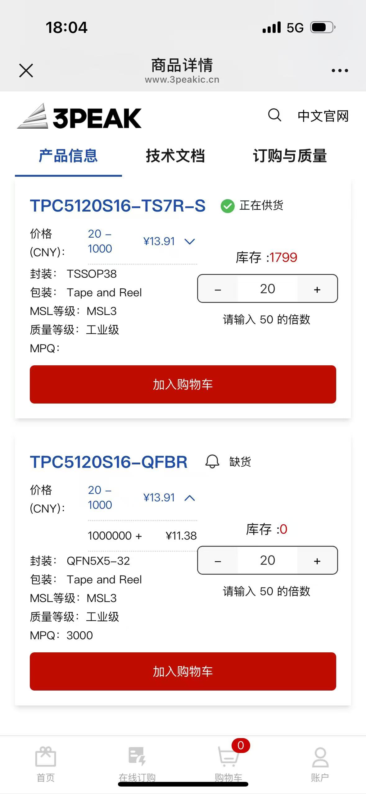
TPC5120 The 3Peak stuff is so promising, but we still have not managed to source anything from them and they won’t work directly with us. I did find a single supplier on taobao for 12kuai, but you never know if that is real, will inquire now. Digikey has it for 24RMB in 100s, szlcsc no longer lists it.

Update: 8.84 12 15kuai. After shuffling through two liar prices it seems we can get it for 15rmb in onesies.

TI ADS7952 (12 channels) and ADS7956 (16 channels) have spotty availability on szlcsc and cost 40-50kuai.

Assuming both chip are similar (previous discussion) here are some things I find interesting:

  • IO pins can run at 3.3volts while the ADC and MUX run at VUSB
  • It is a mux with and ADC, but the ADC and mux are connected externally. This is a great opportunity to buffer with an opamp and /2 so we can use a 3.3/3v reference.
  • “There are two software selectable input ranges (0 V
    to VREF and 0 V to 2 × VREF)” - not fully sure what this means, maybe it has an internal divider? In this case we don’t /2 externally, and then CURRENT_SENSE can also be moved to the external ADC (and be measured against the 3.3v reference)
  • Looking at the protocol, it can probably be managed completely with PIO and DMA, so I don’t need to worry about the shared SPI used with the display and NAND chip.
  • It mentions adding a 150pf cap to each pin to help with settling between channels. Perhaps this is an opportunity to get rid of the opamp on each IO pin without reintroducting “the glitch”.

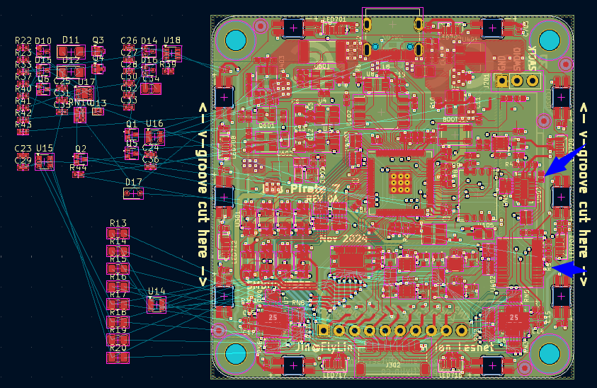
One reason I’m giving this a bit more thought at this juncture: this is what has to be added for the ruggedization or IO and VOUT.

  • The AUX voltage circuit will easily fit int he power supply area near the programming header.
  • VOUT protection might fit in the VOUT area on the top left if the I2C dacs are removed
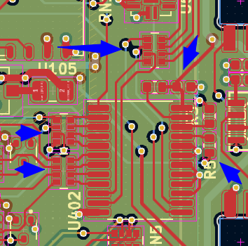
  • In general it is a lot of components to add and we don’t have a ton of space. Removing the level shifter and MUX (blue arrows) and replacing them with a 5x5mm qfn could go a long way towards making everything fit.

Potentially removed pins:
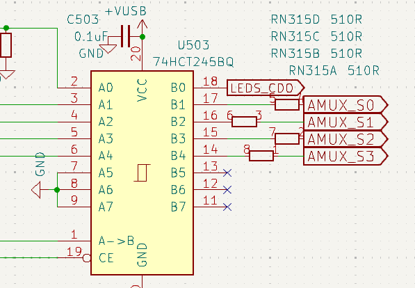
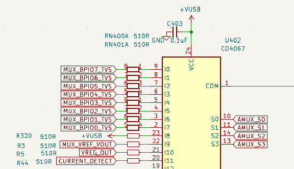
  • AMUX_OUT
  • AMUX_S0-3
  • Maybe CURRENT_SENSE

Potentially added pins:

  • SPI bus

Move slow output signals to XL9555QF24 IO expander

The low hanging fruit (outputs only) looks to be 7 pins:

  • Current_EN_OVERRIDE
  • CURRENT_RESET
  • CURRENT_EN
  • ACTIVATE_VOUT
  • DISPLAY_BACKLIGHT
  • DISPLAY_RESET
  • I2C_RESET (not sure this pin is strictly required, this is a REV0 test)

Kitchen sink

Some ideas I’ve had in the past that might make use of reclaimed pins:

  • A 5-18volt SMPS. This would be super handy in a lot of situations. I discounted it in the past because “where would it output?”, but with the ruggedized VOUT and IO we could feed it to a pin (or pins, with a mux).
  • Infrared emitter and receiver (with minor mods to case tooling using inserts).
  • Your wishlist?

Epilogue

Thank you for following along as I collect my thoughts and make some notes.

When the dust has settled on 7REV1 (shortly, I assume), I will ask our CAD guy if he can fit everything on the board. He usually can, even when I think it’s impossible :slight_smile: I suspect this will be tough though.

If the board is unroutable, we could take a smaller step and then a bigger step:

  • Test REV0 with the new optimized BOM changes and new hardware. If it works, clean off the crud (bad TVS diodes) and make a small batch. Call it BP7
  • Speed along towards a BP8 with SPI ADC and make space for the ruggedizing components. Even without the IO expander, we can score 6 IO pins removing the AMUX. 4 recycled back into SPI, 2 for PWMs to control the voltage and current limit of VOUT.
3 Likes

The board looks beefy. Packed with components on scarse space.

1 Like

My main motivation for looking into this was to free space on the board. The SPI ADC would mean we don’t need all these opamps and muxes anymore, just one ADC IC.

So if your layout expert can make the BP7 Rev1 with the port protection reality as it currently is planned, then perfect. But if the layout becomes too tight then we could incorporate the ADC and immediately get rid of a bunch of chips and free up their space.

It would also improve ADC accuracy and speed of course, but this wasn’t my main motivation.

This could work in a way where you decouple the external VOUT pin from the internal VOUT_VREF with the new protection mosfets. You could then program some voltage with the existing DAC + voltage regulator to be used as IO voltage on IO0 to IO7. The boost SMPS would get it’s own DAC to program the output voltage that would then go to VOUT without interfering with the internal VOUT_VREF.

It would certainly make it easier to work with certain targets that need a higher voltage. But I think we should also duplicate the current measurement + current limiting circuitry we have for the voltage regulator to this new SMPS.

I’m a bit torn if this is really the best usage for the space (and price). In the last few years USB-C PD has become much more popular and widespread. Most USB-C PD chargers now include PPS which allows you to make it output voltages and currents programmed in a very finely controllable way. All you need is a PD trigger circuit. Since all new phones, tablets, whatever are mandated by the EU to use USB-C, this kind of gear will be ubiquitous very soon.

So maybe better create a separate BusPirate PD companion board or something that allows you to easily control a USB-C PD charger with programmable voltage, current, OCP and voltage, current readback. Also LCD to show the data and a graph. I think that would work better than including all the power stuff into the BP itself. Also the chargers usually allow for far more power output than a PC you plug the BP in.

The BP could get a new, dedicated pin header to plug this companion board into without sacrificing any of the existing IO pins. Or the companion board works standalone without the BP and gets two USB-C ports: one you plug into the PC for control and the other you plug into the USB-C PD charger.

Isn’t this better dealt with the IR plank? As you found out yourself when developing the IR plank, there are a ton of receivers of different kinds necessary to decode all the signals. I think the plank is the better solution for this.

1 Like

Codename Power Pirate

1 Like

Excellent point. There are much better, more modern ways to get a >5volts source.

I’m going to focus on this a bit. Especially if you agree that we may be able to get rid of the op-amp buffers. Board space is tight. It would free 10-15% of space, reduce BOM count, and open up valuable real estate near the 10P connector.

The cost of the current ADC components (mux, that DFN level translator, a bunch of op-amps) is 5-6RMB. If the 3Peak part is really available for 15, that is not a small increase, but comes with double the speed. I’d say that’s probably fair trade on a high end board.

1 Like

This is the difference with all those parts removed.

1 Like

I totally agree with @electronic_eel, adding this feels way too “Frankenstein”, Plus, it creates a lot of issues on multiple levels (stock, space, more price…). Keeping it external with a Plank sounds like a better idea.

2 Likes

Even if we are going to use the 3Peak-part, read the datasheet of the TI ADS7952 too. These are so similar that the extensive apps information that TI wrote will mostly apply to the 3Peak one too.

Especially chapter 9.2.2 of the datasheet.

So the idea is that you have a smallish series resistor on the input (behind the main 120R input protection put maybe 330 R, followed by a BAS40 for additional protection of the ADC?), then a 150pF cap and then go into the mux of the ADC. Between the mux output MXO and the analog in you place one opamp that buffers the input. Maybe build an active low-pass filter with the opamp.

This might not get 100% away with glitches when switching inputs, but should solve very much of it. In doubt we can always use a custom channel sequence that stays on one channel for a few samples before switching to the next. When it really matters, like scope mode, we would stay on one channel pretty much all the time to get full throughput.

The input can go straight into the ADC, you don’t need the voltage divider because they have this included in the ADC already with their 2xVref capability.

This would get rid of all the input buffer opamps and so on, just the ADC, the 2.5V reference and one opamp.

Current sensing would still need an opamp for scaling though. One idea would be to still use the ADC of the RP2350 for current sensing. So just the current sensing there, everything else on the new ADC. This would allow to constantly sample the current there without interrupting the new ADC by channel switching. This way we could do continous voltage/current sensing with full throughput. This would allow stuff like a coloumb counter and precise power measurement of the DUT.

1 Like

It appears the 3Peak part can have VREF from 2 to VA, while the TI part maxes out at 3V? I would.really like to keep it at 3.3v for all around ease of integration.

There are several points about the ADC pin protection and power down protection that I’d like to probe. Will dig further when I’m back at a proper PC.

Jin and I meet with some scalpers tomorrow. Ill get some of the 3Peak chips.

I have a better idea how to proceed now, I will post a proposal tomorrow.

1 Like

I think the idea is to use 2.5V as VREF. That would have to be provided from some external reference. The cheapest option would be a TL431 where even the 0.5% ones are very cheap, but there are better ones available too of course. Using a dedicated voltage reference would allow proper filtering and generally better performance than reusing a regulator. And this at just a small extra cost.

When you then use the 2x VREF function of the ADC you can directly sample from 0V to 5V, without needing any voltage dividers.

This would fully utilize the resolution of the ADC. Using a higher ref voltage would waste some of the resolution. Also the ADC seems to be designed to work best at 2.5V.

1 Like

2.5V VREF should be fine if the current sense stays on the RP chip ADC. If not, I suppose we just rescale the current sense output to 2.5volts. There is going to be a lot of cleanup in the code if the VREF changes, but I suppose that’s a good cleanup.

Jin talked to our reliable part suppliers, but nobody can get the 3Peak ADC. There is a single seller on Taobao, and I’ve ordered a handful to test.

My proposal for a path of least resistance:

7REV1

  • All BOM optimizations to date (10uF/6.3V, removing various 0.1uF where not needed, and some gate resisters, etc), reduced component size.
  • USB TVS diodes and 0805 resistors on IO pins and USB pins.
  • Remove advanced VOUT protection
  • Controversially - remove the I2C DACs. We can reclaim one pin from VOUT and one from I2C_RESET (confirmed probably not needed) and stick with the PWM method we’ve been using. It seems like the next version will have free pins and there is discussion above about reverting to PWM in 8, so perhaps not create this separate branch of hardware that relies on a different method.

8REV0

  • TPC5120 1MHz SPI ADC (eliminates a bunch of parts)
  • Use freed board space to implement the advanced VOUT protection

I am uncertain about a few things in this approach:

  • Reverse current/back powering: the ADC has the typical +/-0.2V from rails max rating. To stay within this with a BAS40 I use a 100K resistor, making it quite high impedance. With a 330R resistor will it exceed +/-0.2V when back powered? Maybe the TVS diodes handle this now, but it is not clear to me.
  • On REV8 we had “the glitch”, which was a sag to nearly ground on the IO pins (especially with open drain bus) caused by inrush into the CD4067 during channel switching. I presume the TPC510 has a lot less of an effect (15pF, according to the datasheet?), but I want to do some analysis. The op-amps buffering the IO pins from the MUX are there to prevent glitches in the IO pins, rather than measurement errors in the MUX/ADC.

I find this section of both datasheets a bit ominous, and think we will become vary familiar with it while prototyping.

Chip update

The only TPC5120 seller has now raised the price from 8.4RMB to 30RMB when I tried to buy them. They will take several days to ship, which probably means they don’t really have them or know where to get them. Jin is trying to get samples directly from 3Peak now.

1 Like

Ok, I guess you see issues fitting it all onto the PCB.

The TVS-diodes for the IO pins stay?

Then I would suggest to also put one SMF5.0A on VOUT. This would then give a basic protection for VOUT too.

Yeah, having I2C DACs just for one revision and not the others would complicate firmware.

Maybe we need the I2C-Reset: the logic-part of the TCA6416A is powered with the IO voltage (VREF_VOUT). So should that glitch the parts should theoretically reset themselves. But I do not fully trust this until I have verified that property on a sample.

So I would suggest that we keep I2C-Reset at least for one revison.

Try the approach with moving slow signals to a XL9555QF24 instead?

Ok, seems to be an elusive chip to get. Let’s postpone the detailed planning of the ADC and it’s input configuration until you are sure you can actually get them at a somewhat reasonable price.

1 Like

Jin has exhaustively hunted this part.

The 8.4, 12, 15, 30RMB seller admitted they have no stock and no idea where to get it. The price increase is to cover the cost of their hunt.

Jin contacted the main 3Peak distributor, who was actually very helpful. The screenshot above is from 3Peak’s internal ordering system for distributors. The QFN chip has 0 stock, though the TSSOP version is available. In my experience this means they don’t have in-house ability to package leadless chips, so they require a big order and send the dies to be bonded by a 3rd party.

The 3Peak distributor will contact his product manager to see if we can get samples, and if/when chips may be available in QFN.

Our reliable “scalpers” are not all knowing, but they are well connected in the market and are generally right about their craft. They warned us away from this part and I fear they may be right. Maybe 3Peak will come through though.

VCCP POR

Good point! I missed that VCCP causes the POR. On one hand this is good because we can cycle it, but also adds some complexity to handle when VOUT is changed.

REV0 has the I2C_RESET pin so we will have a platform for testing shortly.

1 Like

Since we now don’t have the VOUT protection logic anymore, we can’t cycle it if VOUT is provided from the outside. So it might very well be that we will permanently need the I2C reset.

Ah, right. We should use that to test this particular issue in detail.

1 Like

Hmm, this means a bit of a production risk - you would rely your whole design and production on one key part that is only manufactured for you.

I can understand why the scalpers warn you about this.

I would make this depend on the reaction and contact to 3Peak. If you can establish a good contact to them and they react in a forthcoming and realistic way then it could work. But if not then I wouldn’t want to take this risk, even if you can get samples right now.

1 Like

The TI part also seems a bit expensive and hard to get online. We’re getting a quote from a few people in the market now. Since it is pin compatible we could experiment with that first.

Another tactic might be to update the CD4067 to a proper 74HCT4067 in QFN? Maybe the input characteristics are improved over the CD4067 and some of the front end stuff wouldn’t be needed? It would eliminate the “expensive” nexperia branded level shifter used to drive the CD4067.

The 5volt world seems to be crumbling away :slight_smile:

Yes, that would also be an option.

What exact mfg. / part number do you use for the first stage opamps? LMV358? Maybe there are LMV324 (or similar part nos) available in QFN too, then you’d need less of them and would save space.

Edit: I mean something like the TLV9004SIRTER:

That is one part in 3x3mm QFN against two LMV358 in 2x2mm each.

Or RT9134GQV:

Or WS72324Q-16/TR:

Maybe we could also move the voltage dividers directly after the first opamps and before the mux:

Use a relatively low-ohmic configuration with something like 560 and 820 Ohms as voltage divider and add something like 47 pF to the output. I guess that would be low-ohmic enough to prevent the glitches you had previously. I would still add one buffer-opamp after the mux though.

But that way the mux would be fully in the 3.3V domain and wouldn’t need a level shifter or be an expensive HCT-part.

Maybe if we combine that with the 4-channel opamps we’d gain enough board space for the VOUT protection?

Adding an IO expander where the DACs were.

Two quad opamps instead of 4 dual.

Using an HCT MUX.

I played around with some of the new parts. While it does feel nice to optimize the board, I don’t feel like it is getting us closer to fitting the VOUT protection circuit. It is, at least based on SZLCSC prices, adding a a lot of extra cost for almost no actual additional functionality.

We should have an actual quote for all these new parts shortly, I will post when it arrives. I am strongly in favor of the quad opamps if it is about the same cost (currently it is 0.6RMB @ 2pcs dual vs 1.35RMB @ 1pcs quad).

Dropping everything into the 3.3volt domain is something I’ve considered over the years, but that’s going to be a mess of passives as well.

I think it may be possible to remove the op-amps, and replace them with a small capacitor that prevents the inrush from glitching the bus.

Let me explain the glitch a bit more because I think we’re addressing different aspects of it. In REV8 there were no opamps or diodes between the IO pins and the MUX, just a simple protection resistor to limit back powering to acceptable levels.

A user’s logic analyzer triggered constantly in I2C mode. Further inspection found that when the MUX changed channels, especially from low to high pin, there was a significant inrush that pulled the IO to ground for a short period. It happens at every 500ms scan of the analog voltages, and looked like steps as it moved from one IO to the next.

One proposed solution was to add a small capacitor behind a resistor to temper the inrush, but I opted to go nuclear and add a bunch of opamps (which still feels like the right answer).

Anyone have thoughts about removing these series resistors?

These are a hold over from before the MUX was buffered with op-amps. They’re 510 Ohm resistors intended to limit max back powering (when Bus Pirate not plugged in, but power is connected to IO or VOUT) to the 10mA listed in the datasheet.

This is one array between the level shifter and AMUX. This is an internal connection and both are powered by VUSB. I don’t think back powering would happen here.

The IO pins are all buffered with op-amps. The op-amps have a resistor and diode to prevent back powering. I don’t think the op-amps will back power into the MUX because they have their own protection.

VUSB shouldn’t need protection because it is the same rail the MUX is powered from.

MUX_VREF_VOUT is protected by an op-amp now.

VREG_OUT shouldn’t be active if the board isn’t powered, and is also protected by one-way switch or VOUT protection.

Current detect is highly unlikely to back power.

I’m pretty sure these can all be removed from the current design.