ok, seems like the XL9555QF24 is the one to go for.
I’m not sure if the NOR-flash in SOIC-8-wide will stay put just with surface tension reliably. And since it is one of the largest ICs on the board it would be a prime candidate to move to the top for saving space.
Won’t make it any easier if you have to change factories for this
On the other hand the VOUT protection is a bunch of tiny passives that would probably stick well, and would require less modification to the enclosure tooling.
Yes, this could work. We’d have to put them on the pin-header side of the LCD though, not next to the USB-C connector. Otherwise routing the signals all across the board would be a nightmare. Let’s hope there is enough space for this there.
VOUT comes from the button side and routes down under the Io buffers. Some parts need to be close to VOUT pin, but I suspect a bunch could go directly over the adjustable vreg near the button.
But, let’s wait to see what happens with the SPI ADC. That will open a lot of space.
I’ve had a few discussions with Supul, who routes our boards, and routing is tight. The additional of the IO pin TVS diodes and change of series resistor location created 8 trances that connect in 7 or 8 places. It’s not that the routing is impossible, but all the vias are breaking up the good ground plane.
We’re discussing some of the same things we’re been over here:
The quad op-amp in 3x3mm QFN may make an appearance.
Current_detect to I2C IO, connect INT to RP2350
The CD4067 TSSOP chip may change to 74HCT4067BQ (DFN), this saves a ton of space with the smaller leadless package. The 3.3->5v level shifter (74HTC245BQ) can then be removed. This does have an impact on the BOM cost. The current solution is about 3.3RMB, while the 74HCT4067BQ is a frightening 5RMB, a 1.7RMB BOM increase. I wanted to avoid any changes here with the massive update to SPI ADC coming in the next version, but it may actually pave the way a bit for those updates.
We no longer have a 1M pull-down when VOUT is not powered, so the leakage through the op-amp protection diodes is a problem again. Floating pins hover at ~2volts.
A super easy change is to add a 1M pull-down to all pins and change the pullx to another value. This defeats some of the impedance (?) testing stuff I imagine.
Second option: an 8bit I2C IO expander powered from VUSB or 3.3V with 1M pull-down on all pins that is enabled at start-up, and disabled when pullx is enabled.
TCA6408A - The obvious choice, but shares the same two addresses as TCA6416A
Will do a bit of searching.
PSU DAC
Working, but it is eliminated in next rev, so I’m not going to mess with it much.
PSRAM
A bit of a mystery to me.
Reset/Bootloader button
I need to get used to it, but sometime the long press still seems to reset instead of bootload. This could be a me issue.
2Gbit NAND
Seems to work, as expected based on @henrygab 's earlier work.
This sounds like you already have received your 7R0 sample? Or do you have remote control to one that is in the China office?
hmm, when is this case an issue?
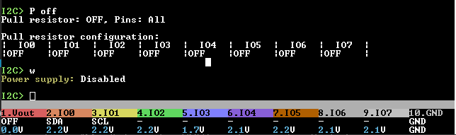
This is just an issue when you have VOUT switched off and you want to use the ADC to measure the voltage on the IO pins. A floating pin will not give you any meaningful measurement result. But the values are shown on the screen, so for users that are not accustomed to this behavior for example from their multimeter, it would be nicer to show 0V.
Or am I missing some real hard issue with this?
I’m not sure if it is worth adding extra components like FETs just for this case. Once we have the Vout protection, we could just power the internal voltage regulator with 3.3V and keep the Vout protection disabled. This would allow to enable the 1M pulldowns, but keep the Vout-Pin off. But you’d then need some extra command to allow powering Vout from the outside which currently is always possible.
Another way to deal with this would be to use a permanent higher impedance pulldown. Is this leakage still an issue if you use for example a 10Meg pulldown?
I’m currently a bit reluctant to use a permanent 1M solution. But I guess I need to work with the new impedance test function a bit to get a better idea how it behaves and how a permanent pulldown would affect it. So I might change my opinion on this point.
Edit: I guess I should have read the other thread first…
Excellent point about the VOUT, that does completely eliminate this whole issue. And the opamps might be replaced by 15pf caps (TBD) with the SPI ADC.
Yes, the floating pins are 100% a cosmetic, marketing, support and UX issue.
The first thing you need to know is that Schottky diodes are leaky and we use them to protect a bunch of opamps that prevent a glitch caused by an ancient analog mux that has a lot of inrush… So your pins are gonna float at 2volts.
I’d budget an extra part in the BOM to prevent this sort of thing I worry about meeting user expectations and streamlining learning. If it were just me I wouldn’t care (that’s probably a lie).
I will conjure up a 10M resistor and see if that is sufficient.
It looks like the board rework opened a bunch of space. I don’t know how much, but we were able to use 8 of the XL9555 IOs to provide the 1M pull-down when VOUT is not active. Hopefully we see the board soon.
I pushed a new branch for 7R1:
Support for XL9555 IO expander
New compatibility layer to handle 74HC595 shift registers or I2C IO expanders seamlessly
Updated pin connections, restore PSU PWM control, other small updates
Nice. And very good to hear that the layout seems to fit in the existing board size without major schematics rework and even more expensive components.
This is a very good thing: Since the XL9555 IOs are full IOs, they also can pull up to 3.3V if you want them to.
So there would probably be the option to replace the 1M pulls on the TCA6416ARTWR with these and use something like 100k there. With 1M the exact voltage used doesn’t matter that much and the risk of destroying something due to too high voltage is negligible.
Another thing that could be added to 7R1: increase the core voltage like mentioned in the clock speed thread. Not to permanent 1.2V, that would be too risky in my view. But a permanent 1.15V should not be too risky and probably something that would enable further speed increase, just like with the RP2040.
So how about changing the LDO to an adjustable one, for example TLV75801PDRVR?
Now that you have the layout you seem to be eager to pull the trigger for manufacturing.
I didn’t have time yet to do the port impedance tests on the 7Rev0 prototype. I will get to those on the weekend or so, but this is just a hobby for me.
But if you want to start production without those tests, then I’d say change the 1M pullx to 100k to give us a broader variety of pulls.
How about the 1.15V LDO? Is there a bit of space for it? The TLV75801PDRVR I recommended should be smaller than the existing SOT-23-5, so the additional 2 resistors shouldn’t need that much more space overall.
After the issues we had with the paste print with the 7Rev0 I think manufacturing and yield will be the biggest issue. You need a proper paste print and AOI (or similar checks) for the paste print to get 0201 or 01005 assembly reliable. And those checks should have prevented the 7Rev0 prototypes going through as they were.
Aside from Henry’s board, I think the main issue in last batch was related to that terrible PSRAM footprint. That’s been replaced with your tested footprint. I have high hopes for higher yield this time. Last batch was highly irregular, we’ve never had issues before.
Point taken about the smaller parts. I will get some info so I understand what a down size involves.
If the PCB is OK, then I want to get the boards made right away. It takes a few days to get 4 layer boards. There’s time to poke at the BOM a bit before PCBA, but understand it’s not on the timeline of hobby interest and that’s fine.
I really want a board with working PSRAM. I also want to build out the XL9555 firmware because I’m almost certain I want to make some tweaks to those connections.
Of course I’d push the board, but I think it’s right to pay the invoice balance due before putting the current draft in git. I’m sorry about that, I had heat/water gyser repair today so I wasn’t fully at my desk.
ack, forgot to add: when the design is somewhat stabilized then doing variants with smaller parts and Henry’s all side LEDs will be an option. So we have space to play around and try different stuff.
My PCBs folder is an absolute disaster of drafts. I think all the changed/new files were pushed, but it is possible I missed something. If you try to load it and it explodes, then it’s probably my fault