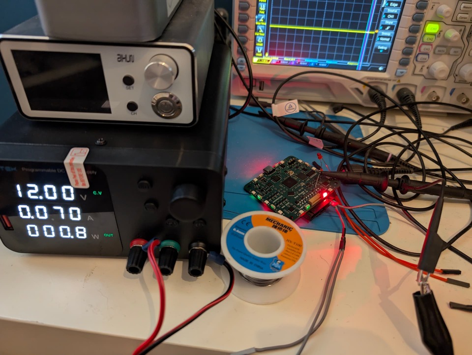
Bench supply arrived! Don’t recommend this one, the interface is awful and it’s bulkier than I’d hoped.
Test setup:
- Bench supply power connected to IO7
- Bench supply ground to common ground
- Scope probe attached to a point behind the series protection resistor on IO7 (yes, that is the lead of a LED soldered on there as a test point).
- Scope ground to common ground
Results:
- Slowly raised the test voltage from 3.3 to 12 volts. Voltage on IO pin stays under 4.1volts.
- Turned the power supply off and on quickly, looking for a <5volt spike with the scope. None found, but the LEDs do come on when 12 volts is applied instantaneously. This did not happen in 1.
- Applied 12 volts for 5 minutes. Measured the temperature of the series resistor (+11c over room temp) and TVS diode (~+8c over room) with an IR thermometer.
- Powered the Bus Pirate and tested IO7: pin works as normal (the scope test was the important bit though).
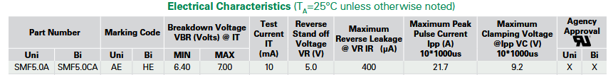
We don’t have full port protection on VOUT yet, but we did add a 5volt TVS diode SMF5.0A.
VOUT test setup:
- Bench supply power to VOUT
- Scope to a point on the board away from the TVS diode
- All grounds…grounded
Results:
- Slowly increased the test voltage from 3.3v to 9 volts. The voltage on VOUT tracked the voltage from the bench supply exactly. I would have expected it to kick in around 7 volts with a big increase in current draw, but didn’t see anything like that.
- Powered the board and enabled the power supply. Initially it showed ~40mA current draw with no load.
- Put the board in the freezer for a while and tested again. ~25mA current draw with no load.
Either something is damaged in the current sense path (false reading), or something is damaged in the VOUT circuit (component actually consuming 25ma).
One thing to consider: the PNP transistors in the back flow prevention circuit are only 5 volt tolerant. It could have been damaged, or failed above 5 volts leaking power back into the voltage regulator which is only <6volt (?) tolerant.
I’m going to investigate further, but as I understand it the TVS is not going to provide full protection but might suppress quick high voltage such as lightening strikes or static discharge. We need electronic eel’s full VOUT protection circuit for more than that.
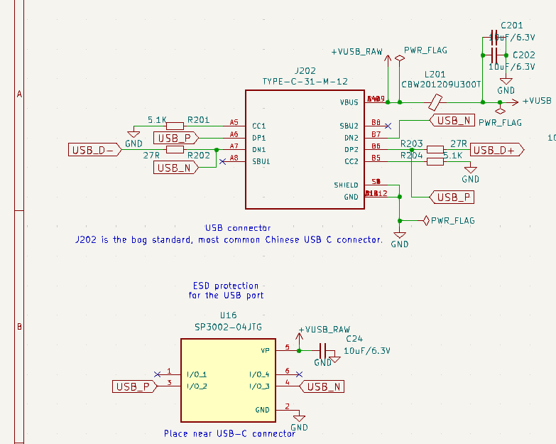
I did not test the USB TVS diodes (which don’t have series resistors) yet.
Findings
Absolutely great news about the IO pins, they seem fully tolerant to a continuous 12 volt supply with minimal heat dissipation. This is a great upgrade from previous designs with minimal additional components.
We already knew VOUT is not protected and vulnerable to some kind of damage > 5volts. It doesn’t stop working completely though, which is a good bit of info to have. Seeing the IO protection in action makes the lack of VOUT protection feel pathetic and totally wrong 
The only issue is fitting the 20ish components for VOUT protection on the PCB. I talked to a few people about it, and we’re going to look into buried vias as a way to increase component density. I’m not sure how much that costs though.
USB TVS diodes not yet tested because I imagine this will be destructive. The TVS diode is placed in the raw USB_N and USB_P pins with no current limiting resistors. I think this is again intended to protect against static shock or lightening strikes (ESD) rather than a continuous over voltage situations. For (somewhat) continuous protection I assume it would be connected after the 27R USB series resistors on USB_D+ and USB_D-. We had this conversation above at some point, and did confirm the current placement.
Next steps
After a bit more testing and debugging, I’ll finalize the next revision. So far there is only one change: over current interrupt to a RP2350 pin instead of the XL9555 I2C expander.
The design seems to be a bit more stable, so this might also be a good time to put through Henry’s variant with all side facing LEDs.