Let’s assume that these libraries work as they should in the SDK-environment they were developed for.
Then something in the BusPirate environment must throw them off. This could be something like interactions between the different cores that you already found out (and worked around). It could also be some MCU peripheral that is initialized in a different way or different order.
You have some experience running other projects firmware on the BP hardware. Is there some kind of reduced, very barebones set of libraries, drivers and initialization you could use to have as few things that could conflict as possible?
Like not initializing the display, the voltage regulator, the NAND, the LEDs, the PIOs and so on? Just the NOR-flash to boot, the USB and the PSRAM.
My 7Rev0 didn’t arrive yet, so I can’t do any testing on real hw yet. But I did a bit of bedtime reading of the datasheet regarding the PSRAM.
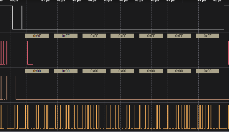
The code in the Sparkfun driver get_psram_size() function looks quite straightforward and I don’t see anything immediately jumping at me that could cause all this 0xff being written instead of the actual command.
Some ideas that you could look into:
DIRECT_TX is a a FIFO with I think 4 words of depth. So if some init-code wrote stuff into it previously but didn’t get to actually pushing it out, this stuff would be written before your new command. Maybe try to repeat writing the id command 4 times to flush the FIFO?
always check the TXLEVEL / TXFULL bits to ensure there is enough space in the FIFO before writing
look at the SD0 pin with a scope. If there is bus contention, as in the PSRAM or NOR-flash driving it high for some reason, you would see a voltage level quite below 3.3V that could still show up as high on the logic analyzer
maybe the security subsystem of the RP2350 interferes somehow. This is a subsystem I haven’t looked into at all yet. But I have seen some access control register for XIP_AUX which seems to affect the direct QSPI access.
thats exactly why i am glad to have a original saleae. if i suspect something like that i can quickly switch a analog channel in in addition to the digital ones.
As best I could, I scoped SD0 with a trigger on PSRAM CS. It did not look like there is contention between chips. However, at this point I have damaged the PCB a bit and attaching things to CS is getting difficult.
I will not test on a PICO2, I forgot the QSPI pins are not broken out and I’m not keen to try to tap them.
Happened to me a few times, too to measure wrong pin. Getting a GND or VCC is more obvious in those cases
Bad connection on a SPI chip is a known issue for me, too. had that once at my computerclub where we debugged a broken BOSE soundbar. final issue was that the MISO pin of the flash had a missing connection ==> firmware load failed and bootfail.
A Spark Fun dev board with this PSRAM is on the way. I’d like to see it actually work with the basic demo, and then try to get the Bus Pirate firmware working on it. Then we know it is a hardware issue pretty much for sure.
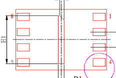
While the PCB footprint does extend the pads beyond the body of the device, the chip itself doesn’t actually expose the pads on the sides. Reheating it with an iron probably isn’t doing much. Hot air rework is a last resort because I might not be able to get it back on.
The default KiCad footprint (top) is way off from what other people are using for this chip. That’s probably the issue. The datasheet doesn’t have suggested paste layer, but this from SnapEDA looks more appropriate (bottom).
I’m a big fan of the new quick press to reset, long press to bootload. The press duration to enter the bootloader is about twice what I expect though. A slow count to three.
Fully agree. It was a very welcome feature (while I used it). I look forward to it continuing to be the default. Next up is to model some smaller buttons, and 3D print them, so I can stack my ever-growing collection.
Looking forward to focusing on this project again soon.
This inits the PSRAM during startup. To see if it worked, type psram on the command line, it should give a size (0 not detected), if detected it runs some memory tests.
All the selftests pass (except the known E9 thing) on my unit, the NAND flash works and the bootloader button also. The SMD soldering looks fine on my unit. Only the SWD header is tilted a bit. But this is the hand soldering of course, totally different thing than the ugly blobs around the RP2350 on henrys unit.
Yes, the footprint seems to be way off, the pads are much too long.
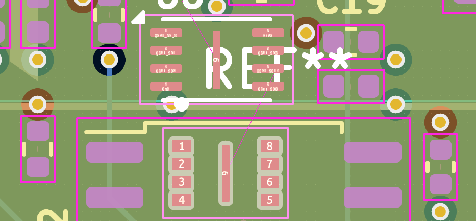
I have used the Winbond NOR flashes in exactly this USON 8 / 3x2mm package that the PSRAM comes in on like 400 units now over several batches, PCBA at JLC. Not one issue with soldering the flash yet. Since I didn’t like the default Kicad footprint I created my own. You can use it if you want.
I just hand-measured mine and the bootloader seems to trigger after just a bit over 2 seconds. This is quite shorter than what I’m used to. Yours sounds to take longer.
To me this sounds like there is quite a bit of difference between the units, and maybe temperature. The circuit is optimized for simplicity and not precise timing. It very much depends on the threshold of the FET, and that is something known to vary with each unit and temperature.
The question is if this is ok for this application. I’d say yes.
If not, the two FETs could be replaced by one 74LVC2G14 plus two diodes. Same part as in the VOUT protection circuit. This would give a much better defined threshold, but still be reasonably small (SOT-363).
I just drilled a hole in the case for easy access to the button. I have to say I really like the new case. Much better look & feel than the old one. Also properly sturdy material when drilling.
I found an issue on my unit but don’t know if I also got some solder blobs, äh, easter eggs, to search or if it is a firmware issue:
The current limit always triggers if set:
I2C> W
Power supply
Volts (0.80V-5.00V)
x to exit (3.30) >
Maximum current (0mA-500mA), <enter> for none
x to exit (none) >
3.30V requested, closest value: 3.30V
Current limit:Disabled

Power supply:Enabled
Vreg output: 3.4V, Vref/Vout pin: 3.3V, Current: 1.2mA

I2C> w
Power supply: Disabled

I2C> W
Power supply
Volts (0.80V-5.00V)
x to exit (3.30) >
Maximum current (0mA-500mA), <enter> for none
x to exit (none) > 100
3.30V requested, closest value: 3.30V
100.0mA requested, closest value: 100.0mA

Power supply:Enabled

Error: Current over limit, power supply disabled
There is nothing connected to Vout and it doesn’t seem to actually draw excessive current. Injecting a voltage from the outside also works without issue and unreasonable current draw.
So it could also be just the firmware creating the wrong voltage for the comparator or something similar. Or was this the point where you didn’t implement the full I2C DAC stuff because we planned to not continue using them?