SparkFun - Basic PSRAM Test - starting
PSRAM setup complete. PSRAM size 0x0
PSRAM not detected - done
1 Like
maybe get out the logic analyzer and take a look at what is going over the wires?
When I played with directly (=without XIP) accessing the NOR flash on the RP2040 I had some issues with timing. Only when I lowered the SPI speed on the RP2040 I could get it to work reliably. Maybe it is something similar here? Is there a clock division ratio config variable in the driver that you could increase?
1 Like
Thank you so much for confirmation, that is super good to know.
Tested this at half, quarter, and 1/8th speed, but the result is the same.
Yup, the unavoidable next step. Clipping into the SIO0-3 on the SOIC chip is thankfully easy, but attaching CS is going to need some hot glue reinforcement.
1 Like
I’m time-constrained this weekend, so no probing. I’ve taken pics from a Plugable USB microscope; Something seems off with at least RP2350’s solder?
USB ... not pursuing
USB connector seems solid.
I’m calling the USB zero-sized device descriptor as unrelated to BP7r0. I’ve seen this issue before, so it’s either a latent firmware issue, or it’s related to USBIPD. I’m guessing it’s USBIPD. Either way, I can’t dig in for now.
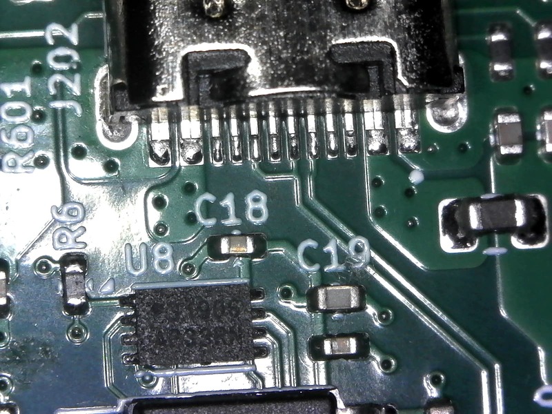
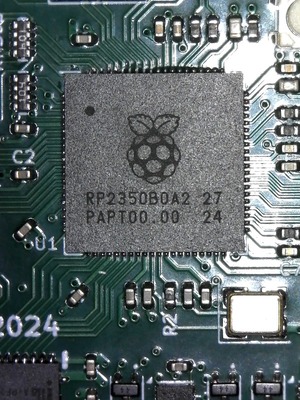
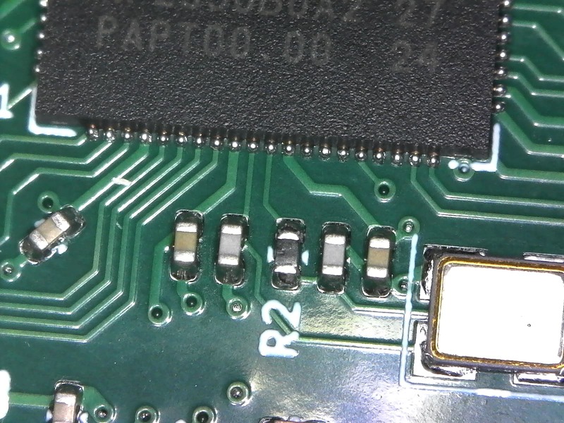
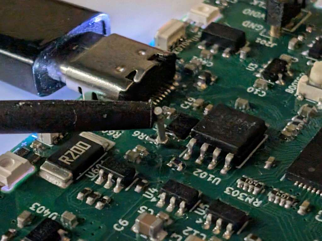
Visual inspection of BP7r0:
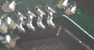
I don’t know which is “better”, but there’s definitely some variability in the solder on the RP2350. Pins 1-70 have blobs that remind me of cold solder joints, where I didn’t heat the board enough, or maybe too much solder? Pins 71-80 look like I’d expect (best seen in oblique view).
Full-sized PNG images (discourse downsampled and converted to lossy JPG format … so …) are available as a ZIP file or view web share.
2 Likes
The solder along the top side of the chip does look a little bubbly. I would hit that with some flux and clean it up with a wick, but I don’t actually see any bridges.
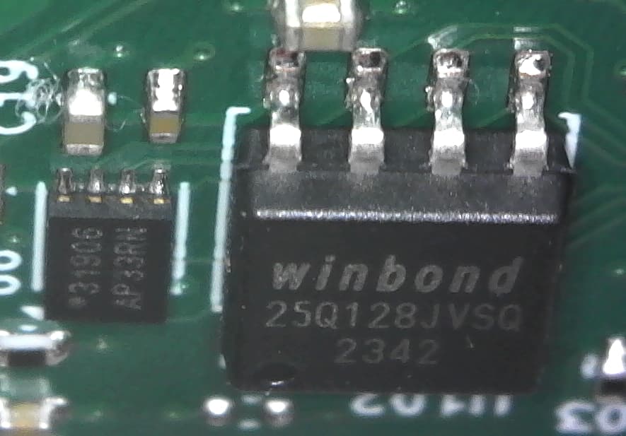
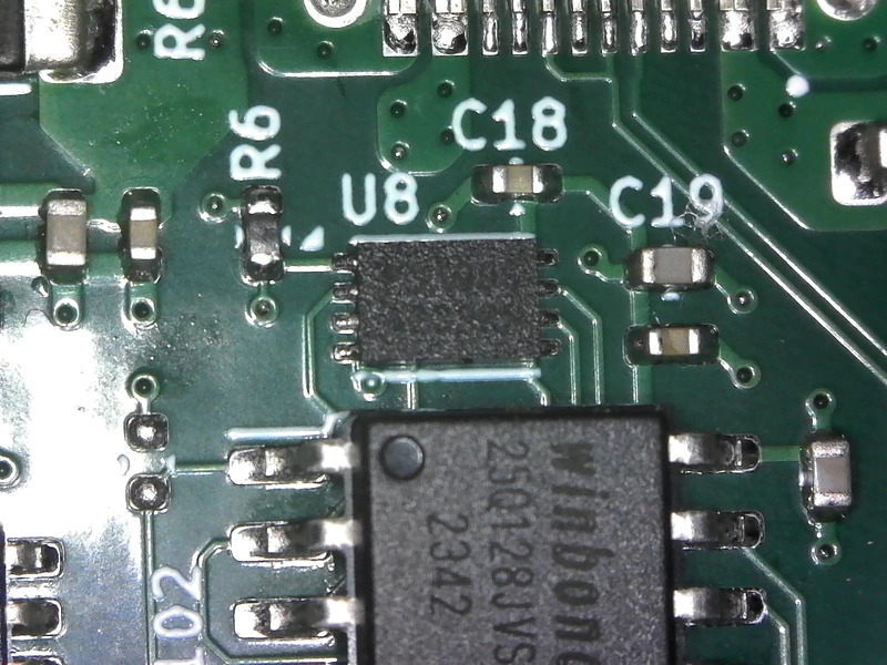
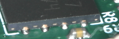
The nand chip is to the right of the RPi chip, the big flat leadless chip labeled U105. The leads are super far apart so bridges are highly unlikely. It could be a soldering issue though.
The NAND and LCD share the SPI bus. If the LCD works then MOSI, CLK must be okay on the RPi chip. That leaves MISO and Flash_cs as potential issues.
1 Like
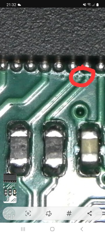
@ian What is the CS RPi pin for the PSRAM ? 58?
1 Like
GPIO47.
There are four available pins for this function.
As far as I can tell @Alex did his version with the Bus Pirate firmware with same pin, So it should be correct/possible. I will verify with a logic analyzer tomorrow first thing.
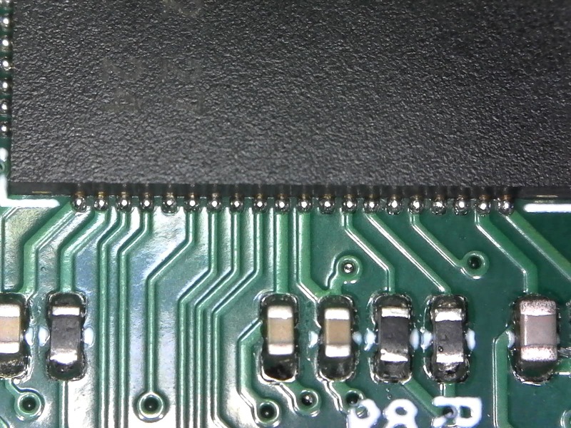
Thanks for posting the closeups.
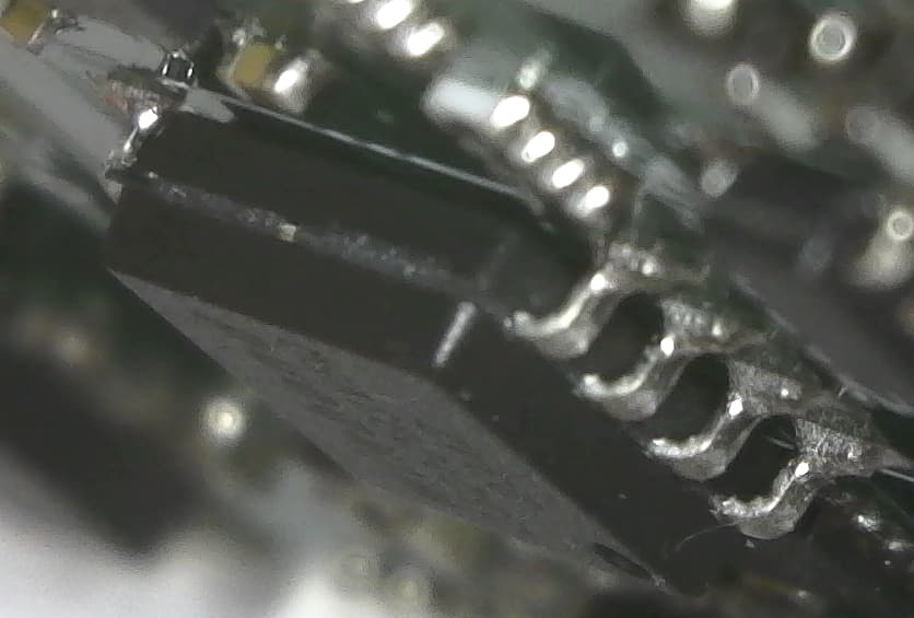
While I can’t see any obvious shorts, I think I can see some small solder balls between the pins and around the RP2350:
When these are on the outskirts of the IC, they could very well also be under it and cause a short there. So I’d think once you have the time doing some probing on the RP2350 side would make sense.
To me this huge variation in solder blob size between the left and right size in the picture looks like there was some issue with printing the solder paste. So the issues we have seen on the other 7Rev0 must not be the footprint for the PSRAM, it could be some process issue while printing the paste, affecting different areas of the board.
1 Like
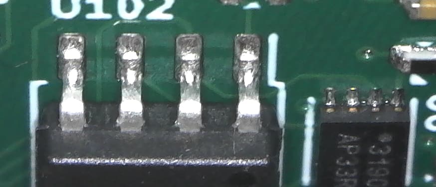
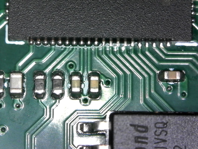
Could be here too. Those are the USB pins.
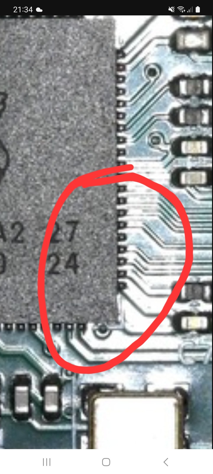
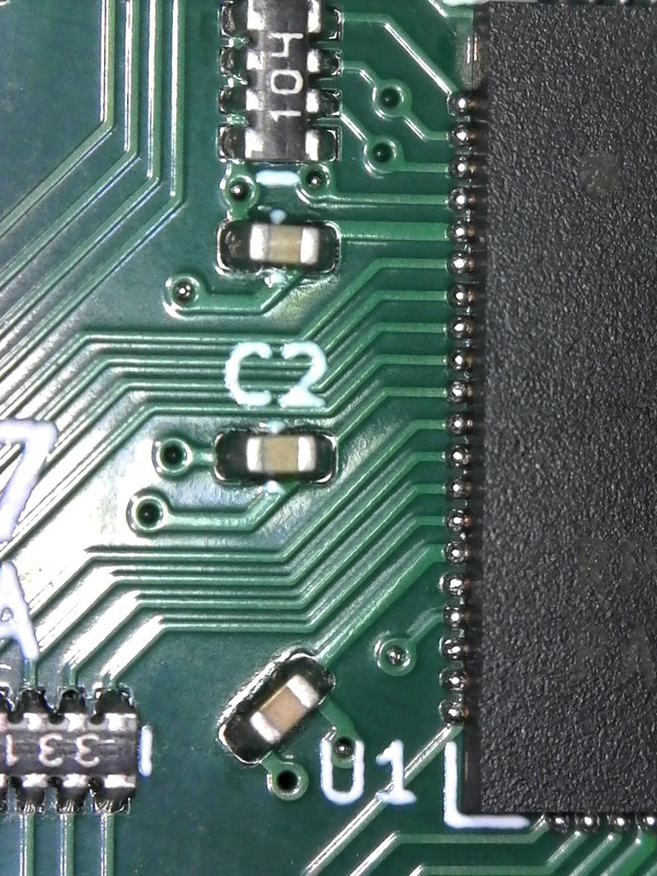
This is the SPI corner, it looks OK.
If I had it on my bench I would hit it with flux and blindly hit the sides with wick. I realize not everyone is equipped for this, I’m definitely not pushing it.
1 Like
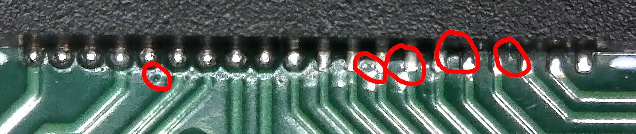
I’ve hit the chip with flux and copper braid, and all the balls are gone, leaving what I would have expected. Pins 71-80 still are sparser than the other pins.
This didn’t resolve the on-board storage … it still does not format / lists nothing. However, looking at the correct chip showed what might have been (one of) the problem(s).
Closeup of the NAND
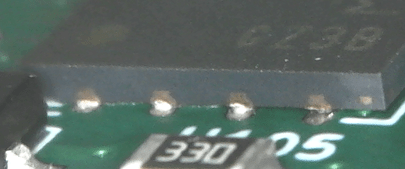
Touched solder to that pin, which should not have solid connection. Sadly, did not resolve the on-board storage (format fails identically).
If want me to check continuity (maybe possible late tonight)...
I’m not a EE, but I can count pins and follow instructions about as well as a trained ape. If wanting me to check continuity (unplugged) anywhere else, please give me explicit instructions, maybe similar to the following?
| BoardID | Pin | Friendly Name |
|---|---|---|
U1 |
38 |
Foo |
U9 |
3 |
Bar |
Continuity Tests:
-
U1 Pin 38(Foo) against adjacent pins -
U105 Pin 4(Bar) against ground
Or, maybe I’ll just be done with 7r0. Leaving it plugged into USB, it rebooted with no interaction. That’s a bad sign, and I don’t want to fry anything (e.g., my PC).
3 Likes
Thats probably the right course of action given the conditions. Get that pin soldered.
I’ll send you a new one and have them inspect that better.
If it won’t “wet” (take solder) then I’d hit it with the least offensive smelling nail polish remove you have access to. Or a rusty bottle of acetone if that is allowed in your residential situation.
1 Like
No need for a new 7r0; I have a bunch of Pico2 boards (13 left) that are letting me mess with the OTP directory stuff. I’m leaving them in non-usable states less frequently now, so I probably won’t run out. That’s where I think I can provide greater value … the software side … the hardware side I’m just barely competent, and have dangerous knowledge gaps. ![]()
2 Likes
I’m just really sorry I mailed out a bunch of broken proto boards ![]() We’ve not had this problem with any of the other Bus Pirate prototypes this PCBA made for us.
We’ve not had this problem with any of the other Bus Pirate prototypes this PCBA made for us.
2 Likes
better to catch that in a proto run than in mass production though…
3 Likes
Was not looking forward to tapping the PSRAM CS, but then I remembered the custom milled test point pins we made last year. Nice grip with just a few seconds of soldering.
Chip was looking messy, so I cleaned it up with finger nail polish remover. Then I hit all 8 pins with a bit of flux and extra solder.
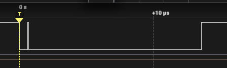
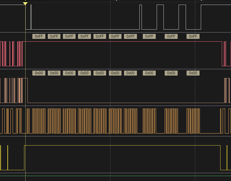
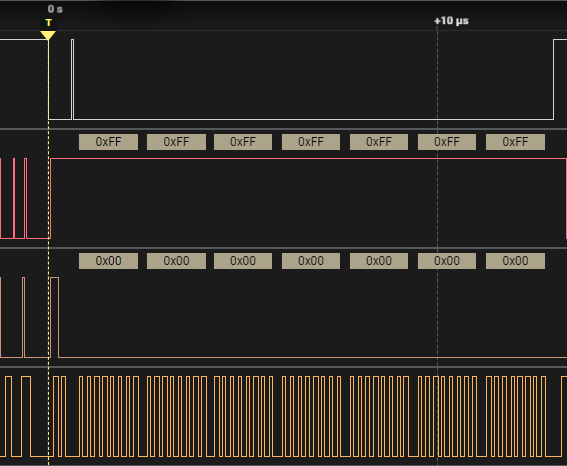
I only have time for a quick peek at the CS pin right now. It is held by a pull-up resistor, so it should stay high unless the RP2350 pulls it low. It is wiggling, and with consistent timing.
Next I’ll need to connect to the 4 data pins and see what’s being send/replied.
2 Likes
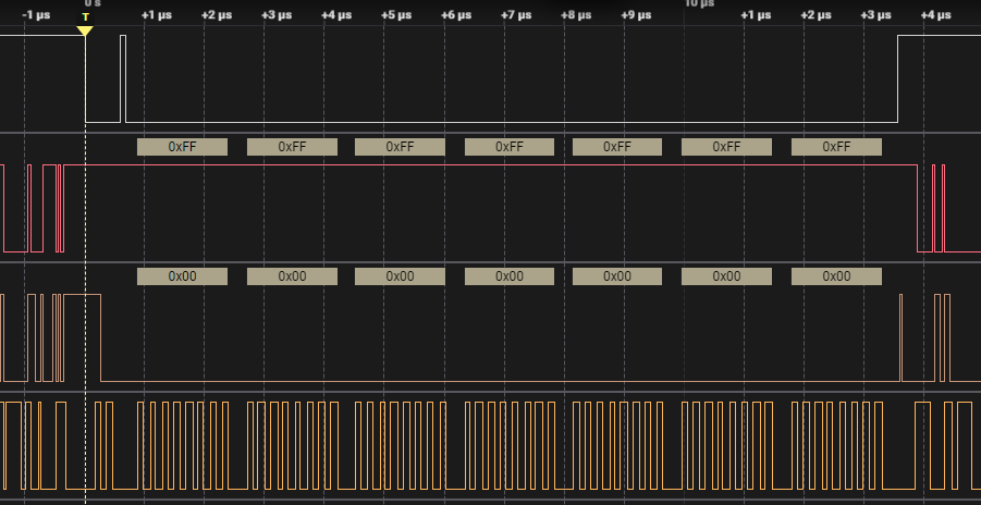
    // Transmit the command to exit QPI quad mode - read ID as standard SPI
    qmi_hw->direct_tx =
        QMI_DIRECT_TX_OE_BITS | QMI_DIRECT_TX_IWIDTH_VALUE_Q << QMI_DIRECT_TX_IWIDTH_LSB | PSRAM_CMD_QUAD_END;
Guessing the first CS low is 2 clock ticks (8 bits) in QSPI to exit QSPI mode.
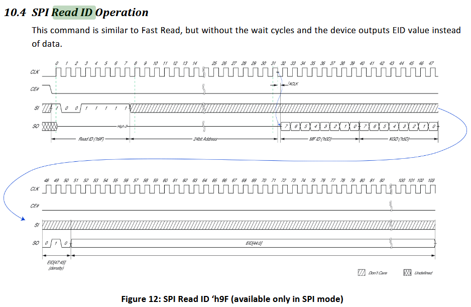
const uint8_t PSRAM_CMD_READ_ID = 0x9F;
    // Read the id
    qmi_hw->direct_csr |= QMI_DIRECT_CSR_ASSERT_CS1N_BITS;

    for (size_t i = 0; i < 7; i++)
    {
        qmi_hw->direct_tx = (i == 0 ? PSRAM_CMD_READ_ID : PSRAM_CMD_NOOP);
Then we do another CS:
- Write 0x9f read ID code - this is not happening, it is sending 0xff. This is probably the hint, something about our NOR FLASH config is off?
- Write NOP (0xFF) for 6 cycles to read the ID code
– 3 bytes dummy address bytes (0xff)
– 3 bytes to get ID info
7 bytes are being read, but the first byte should be 0x9F, not 0xff.
That seems to be the issue. The cause… needs more debugging.
2 Likes
qmi_hw->direct_tx = 0x00; //(i == 0 ? PSRAM_CMD_READ_ID : PSRAM_CMD_NOOP);
Even if I force the value transmitted to 9f or 00 the logic analyzer still shows ff.
2 Likes
What about the CS of the NOR flash while running these commands? Is it properly off or are both chips activated at the same time, resulting in a clash?
2 Likes
Good thought. NOR CS looks okay.
This is using spark fun’s example firmware with only the CS pin changed. Same issue.
1 Like
I guess the next step is to load it on a pico2 and see if the correct commands are sent.
1 Like