I’m very to learn more about this, and I will have a look at PSRAM this weekend.
1 Like
The flash chip is NOR, not NAND like the rest of the BP5+ family? I think we have to revise the Dharma layer if it is the case…
2 Likes
HiZ> ls

HiZ> format
Erase the internal storage?
y/n> y
Are you sure?
y/n> y

Formatting...
Error: disk errorError: Format failed...
Error: disk error
HiZ>
1 Like
Moved @Alex 's work from here on PSRAM support to the 7r0 branch.
PICO_RUNTIME_INIT_FUNC_RUNTIME(runtime_init_setup_psram, PICO_RUNTIME_INIT_PSRAM);
It freezes during start up, due to something in the ‘runtime_init_setup_psram’ which is tied into runtime init like so. If you’re using the 7R0 branch for something else, comment out the runtime_init_setup_psram function to prevent freezing (or maybe this is just a my board bug ![]() ).
).
I will look into this tomorrow if someone doesn’t spot my likely very obvious bug before then ![]()
I created a psram command that attempts to allocate, fill, and test two chunks on memory.
The ‘disk’ storage is still NAND on the internal SPI bus (no Q). The firmware is burned to a NOR chip that shares the QSPI bus with the PSRAM chip. I think the intent was to suggest that the bug is one of three chips on the QSPI bus: RP2350, PSRAM or NOR flash.
Thank you, that is quite clear.
1 Like
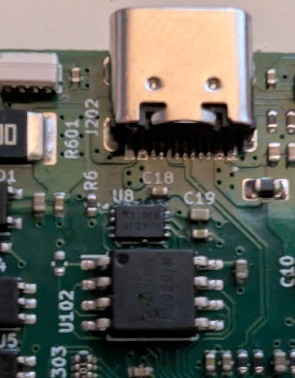
The resistor from the PSRAM CS(1) to 3.3V isn’t there and it is marked at DNP on the PCB file of the 7REV0A
2 Likes
1 Like
Oh, I get it. I confused the chips. I have been looking at the wrong one all along.
Pin 2 are tied for both chips so the 2.2V measurement is still valid. Now I need to check the voltage of CS of the PSRAM. I see the resistor installed…
Sorry about the mis information. The CS pin voltage is 2.2V as well. I see that Pin1 and Pin2 of the PSRAM are tied together (continuity testing while the power is off)
3 Likes
So it could be a solder bridge on psram pin 1 and 2?
2 Likes
I think I see it under the microscope. It is right under the chip. I see a metallic reflection between the 2 pins right at the edge. Not sure I can do anything about it… I can try to heat up both pins and hope the bridge decides to break on its own. It isn’t really reachable
3 Likes
If you are able it seems worth the effort to hit it with some flux and heat with an iron to see if it will reflow back into place. I’d go so far as wicking a bit of the excess with some.copper braid.
In the photo it looks like a lot of solder on my chip as well. The stencil probably needs a tweak.
2 Likes
OK fixed… The log press works correctly now. I need to clean the flux and I am done! Yeah!!
5 Likes
Nice work!
I will check the footprint and paste layer to make sure it’s right. It does seem like excess solder.
1 Like
The problem is that the chip does not sit on the PCB, it is off on the side pin 1 -pin 8 because there seems to be some debris there. I think this allowed the bridge to happen
2 Likes
Sorry to have wasted you guys time because I confused the function of chip U8 and U102. Thanks for the support!
3 Likes
It’s a barn raising and I greatly appreciate your participation. Nothing wasted.
We now know the cause of a really weird issue that could crop up during manufacturing, which is good as gold.
I checked the footprint and it is accurate to the datasheet dimensions, but the datasheet doesn’t include a recommended paste aperture. In this case we tell the assembler and their stencil maker gives that spot some attention. There is a tiny center pad under the PSRAM, and I wonder if too much solder there caused the chip to tilt as you mention.
2 Likes
It is possible. I see the black plastic debris wedged between the PCB and the chip near the PIN1, It may have gotten there after the soldering due to the chip being lifted off the PCB.
2 Likes
Very good that you found the solder bridge. And right at the spot I first thought it might be at ![]()
Now we just have @henrygab s NAND and USB issues left. And anything that I might find once mine arrives.
2 Likes
@henrygab do you happen to have some time checking your 7Rev0 for shorts near the NAND flash?
Even though the NAND flash is a much larger component than the PSRAM, there could still be shorts between the pins there and be the root cause of your NAND flash issues. Also the short could be on the side of the RP2350, so also check the pins 38 to 45 there (RGB_CDO, DISPLAY_BACKLIGHT, DISPLAY_RESET) against the neighboring pins that go to the NAND flash. Also the short could be to GND on the exposed pad underneath the RP2350.
1 Like
Switched to Spark Fun’s pico support for PSRAM, which looks like what Alex used but requires to be installed as a library in the pico-sdk folder.
static void main_system_initialization(void) {
    system_config.psram_size = sfe_setup_psram(BP_PSRAM_CS);
bus_pirate7.zip (301.8 KB)
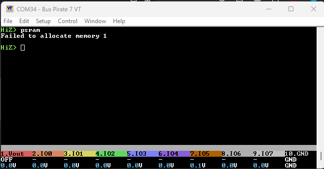
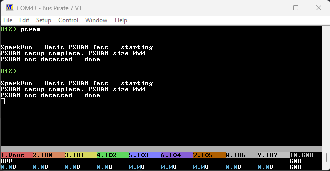
At first this also resulted in freezing, but then I moved the setup to the very top of system init (before core 1 is activated, I think this is the issue) and it boots normally. However the PSRAM is not detected.
To try: load this firmware, then use the psram command.
has_psram.zip (27.6 KB)
To double check I modified and compiled the has_psram example, and it also does not detect the PSRAM. WARNING: this test starts after a 2 second delay, so have your terminal ready to auto connect.
Inspecting the board I notice a few things:
- A stray solder ball stuck in flux between the PSRAM and NOR flash.
- Lots of flux residue, I believe this part was reworked during assembly, more evidence of a bad footprint paste layer
- Poorly looking solder job
I’m going to clean up the PSRAM a bit and try again.
EDIT: cleaning up the solder did not help.
1 Like
Managed to get the self-contained version of the PSRAM driver to not freeze on startup by reinstating bits from the sparkfun version.
PSRAM is still not detected though. Current progress posted to git.
1 Like