Bus Pirate programming/debug rig


There was a discussion earlier this week in the live chat about programming/debugging the Bus Pirate. The 2.54mm 3 pin header on the bottom is used for JTAG debugging, but it is a low profile milled type that mates with “fancy” milled header. This makes it a bit awkward to debug without buying the specific header.

I did make a 3D printed debug station, but the 3D printing isn’t accurate enough and the pins are a super huge pain to insert into the bottom of the Bus Pirate.

After our discussion I drafted an acrylic and PCB based debug rig. I don’t really have time to follow through on that at the moment, so we did the proper thing and contacted a test rig designer. @jin found someone that was willing to do the design, and release all the files to us so we can make it into a kit.

A few days later, called “Shenzhen Speed” in China, we have a draft design. I’m absolutely thrilled that it’s the very specific orange color (POM?) used on almost all the test rigs I’ve seen. However, that might be really heavy and $$ to ship.

Here’s a translation:

  • An acrylic bottom
  • PCB that holds socketed test pins
  • Acrylic layer to support the pins and hold the Bus Pirate
  • Copper standoffs

I’m really pleased, and the price was really surprising.

5 Likes

That just opened up my weekend. I was preparing to print and assemble a few jigs to see if the tweaks I made would help. Thanks again! You knocked that out quick, as usual.

3 Likes

I mostly understand the schematics, but I’m not entirely clear what the PCB layer is doing. I presume this jig helps make quick and reliable debug connection with the Rev10 board.

With the USB-C connector being at right angle to the debug connector, and the debug connector lacking power, am I correct to presume the USB-C connector is attached to the BP5 first, and then the entire case is hand-pressed onto the jig?

Is the PCB on the jig holding POGO pins (or other sping-loaded connectivity), longer-than-normal “fancy” milled header pins, or standard pins? (my guess is extra-long “fancy” milled header pins, since the diagram appears to suggest use of 10mm spacers on the PCB?)

Am I also correct to presume that there’s no top layer that presses on top of the BP5 to hold it in place, since there are no POGO pins?

1 Like

image

There will be a TEC183 or similar spring loaded retaining clamp.

I requested socketed pogo pins, because they do tend to bend or wear out.

3 Likes

This has kind of gone off the tracks. We’re on the third test rig company :slight_smile: Each starts out with a lot of bravado about the previous not knowing what they’re doing, only to not be able to pull it off either. It’s just not clicking.

I may take another stab at it over lunch, we’ll see.

/hangs_head_in_shame :slight_smile:

1 Like

image

A really quick, really poorly done model, without a retention clip.

  • P100-E2/E3 pogo pins
  • R100-3T pogo pin sockets (middle layer of acrylic secures socket, PCB (red) solders socket tails)
  • 4 layers of acrylic:
    – Top layer 3mm or 5mm, with cut for USB (to be done)
    – Second layer for supporting Bus Pirate and aligning pogo pins
    – 3rd layer at retaining ring height of pogo sockets
    – 4th layer for base support
  • PCB to solder pogo pins, with 2.54mm header off to side
  • Using HEX standoffs and with the nice rubber feet that are going on the RS-232 plank

BusPirate5REV10-debug.zip (4.8 KB)

Here’s the OpenSCAD script. it’s just hacked onto the bottom of the Bus Pirate enclosure model. It needs to be updated to calculate all the variables properly and give a report of the spacer heights we need. Also, some kind of unobtrusive retaining clip.

1 Like

I printed this design and am waiting on pogo pins and sockets to get a feel.

Screenshot_20240810_194840

I remember that these chunky guys are used to support the four corners so the pogo pins don’t take the brunt of the force. Ordered several and several sizes of POM spacers that screw into the M3 version.

Screenshot_20240810_194850

The retention mechanism has been elusive, but these seem to fit the space available in the rig without weird wings off to the side. Not as cool as a lever release, but keeps the cost way way down and should be effective. Worry a bit about stressing the acrylic, so I’m getting a few support components as well.

2 Likes

Oh, should I just put an RP2040 and USB C on the PCB so no external programmer is required? Can have a simple header too. Doing a fully integrated thing would be nice, but it also will need FCC and CE testing.

2 Likes

Are you intending to sell this, or is this solely to help flash them in production?

If selling, are there that many folks who’d want/need to drop many devices into a programmer? (If it’s not as simple as dropping into a docking station, consider how this benefit the user vs. just using a Pico Debug Kit with a 3-pin milled pin connector.)

If very few to be sold, would selling it as a “kit” (e.g., “solder RP2040 Dev Board X here”) avoid the need for FCC/CE testing?


Other thoughts on reducing steps / improved experience

If this is intended for average developer folks, it would be beneficial to be “one step” / “one motion” to insert and use, which means it would likely need the debugger integrated. However, if I understand correctly, the debug / POGO pins cannot provide power. Thus, there is a need to plug in USB-C for power (even if not using it for data).

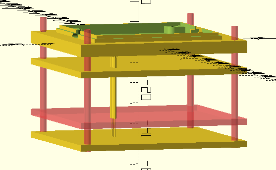
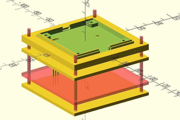
The USB-C connection is orthogonal to the plane for the debug pins. This makes it much more complex to have a single, linear motion for an encased BusPirate that will connect both the USB-C connector AND the debug pins. However, that’s the goal, as the best experience would be where the user leave the cables connected to the dock, and only inserts/removes the bus pirate.

If the BP boards were revised to have the debug port on the same side as the USB-C connector, a dock would be fairly easy to make, and a single motion would easily connect everything. But, that needs both a board and case revision … not a great option, and it wouldn’t support any existing boards / cases.

Slightly more complex, I can imagine a docking station style solution, where the POGO pins will drag along the back side of the case slightly until they “click” into place. This requires moving parts:

  1. Imagine the Nintendo Switch’s docking station (simply because it has USB-C at the bottom), but of course narrower screen-to-back to match the BP5 case dimensions, and with sidewalls to help align the USB-C connector.
  2. During the last ~10mm of pressing the BP5 down into the docking station, the BP5 case engages a spring-loaded lever.
  3. The lever’s action causes the POGO PCB to be brought closer to the docking station.
  4. The POGO pins might initially make contact with the back of the case, in which case they would slide along the back until the case is fully inserted.
  5. The POGO pins eventually make contact with the debug connector.
  6. Removal: Requires the POGO pin shape to allow the POGO pins to detatch from the debug connector with sideways force… then sliding along the case until the lever action retracts them sufficiently.

A more complex action would move the POGO PCB in lockstep with the pushing-down, while simultaneously closing the gap between the PCB and BP5. This more complex action would remove all strain from the POGO connectors, but … requires some maths to design the level action correctly (well beyond my ken).

Not terribly complex, but definitely more likely to wear out the POGO pins more rapidly, depending on the lever’s motion … likely want the lever to cause little/no change in distance initially, and then bump up fairly rapidly near the end.

I’ve no mechanical training, so likely many things above might not work perfectly, or require unrealistic tolerances, etc. Just some thoughts that start with the improved experience that makes it helpful to the random developer, then working backwards towards how that might be done.


1 Like

For newer reversions it might be better to use the default debug connector that Raspberry uses and their debugger comes with the appropriate cable for that connector

1 Like

Just my opinion, of course: I would vote against a change to the BP to use the default debug connector that Rasperry put on. The RP2040 debug connector is small, and difficult to remove once inserted.

Although not as common as standard headers (likely due to cost), machined pin headers are more common than the RPi debug connector. More than that, the machined pin connectors are really nice to use, with solid tactile feedback on insertion. After getting the corresponding part, I really like the machined pins.

1 Like