Parts are sourced. We’re doing three prototypes, which have a 2x10p pin header instead of a keyed IDC connector. I’ll send one each to @henrygab and @kd7eir to confirm it works, and also the direction&pinout for the IDC connector.
An issue I didn’t consider: the 3P milled pin header has about 3mm of stand-off from the board.
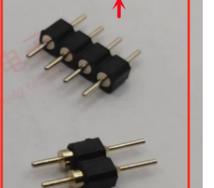
- Bottom type (what I have) has an additional metal stand under the plastic material
- Top type (on order) does not have the additional stand and is about 3mm tall. This is what we sourced for the board.
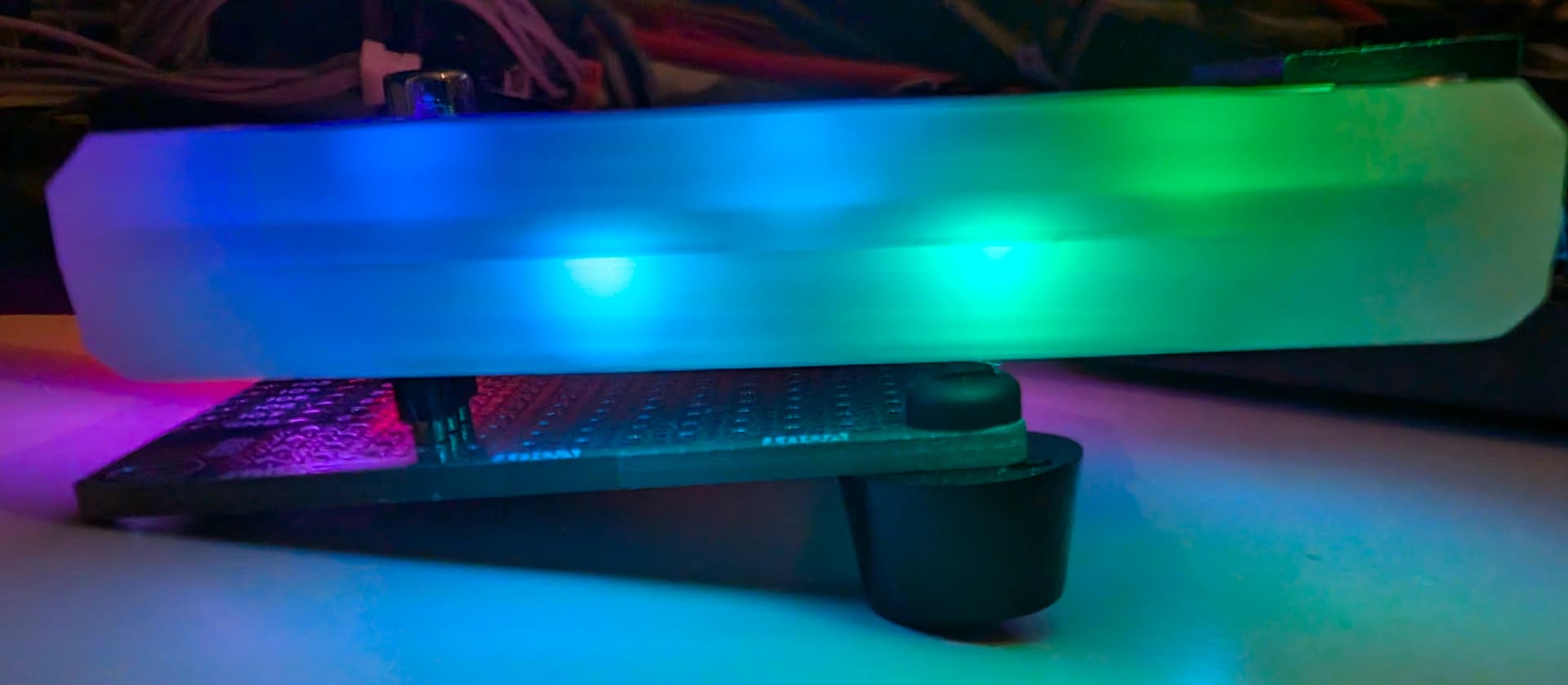
This is an example with the extra metal stands. I’m not sure what to do about this. It kind of circles back to needing a cradle and eventually changing the programming connector type.