Ok, will send out the gerbers tomorrow and get it going.
1 Like
I’m definitely interested.
1 Like
Hi Ian … easy questions / low priority
-
Are these boards going to be populated?
- If not, can you add a “parts” option corresponding to the schematic’s BOM? (With machined pins for debug connector, of course!)
-
Similarly, are the protoboards shipping w/o the SMD parts populated?
- If so, having a “parts” option there would also be appreciated.
Why? ...
I tinker, but I don’t often use SMD parts. I imagine the cost you’d have to charge for a small bag of parts would be less than I’d have to pay for shipping a single SMD resistor from Digikey / Mouser / Arrow / etc. I mean, for the “Fix Your Six” thing, I bought 50x of the resistor packs, and the parts cost was still dwarfed by the shipping charge. ![]()
2 Likes
It’s not much, the cost will be in doing low volume. The assembly cost at low volume is 18rmb ($3) a board.
1 Like
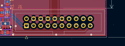
Can someone with a JLink please confirm if the orientation of the keyed connector is correct here? It might depend on the specific IDC cable as well. I could just populate the first prototype with plain pin header so it works either way.
To more thoroughly answer your questions:
Are these boards going to be populated?
Yes, this board will be populated.
Similarly, are the protoboards shipping w/o the SMD parts populated?
I wasn’t planning to populate them or include parts. I assumed that folks who buy prototyping boards have part books/bin/etc. It would be a negligible cost to add a 0805 R/C/D, but is that useful or just more e-waste?
2 Likes
As always, I will defer to your knowledge of the market. I only share my personal desire for things. Glad the JLink adapter will be populated!
- Yes, I can confirm that a standard 20-pin IDC connector is used with the JLink, and that the orientation you used works well. The cable will lie flat in the following configuration:
    +-------+
    |       |              /---+----USB-----+
USB | JLINK |=====IDC =====|x  |            |
    |       |              |x  | BusPirate  |
    +-------+              \---+            |
                               |            |
                               +-||||||||||-+
I’d really prefer an IDC header. The key just removes one more source of user error, and I need all the help I can get. ![]()
1 Like
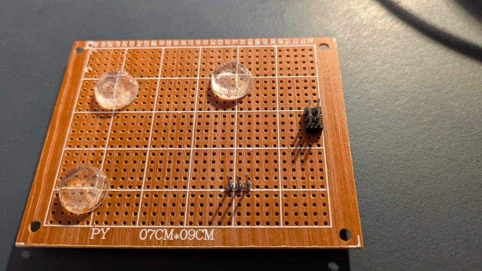
Parts are sourced. We’re doing three prototypes, which have a 2x10p pin header instead of a keyed IDC connector. I’ll send one each to @henrygab and @kd7eir to confirm it works, and also the direction&pinout for the IDC connector.
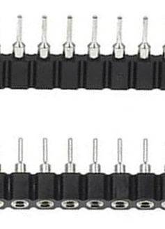
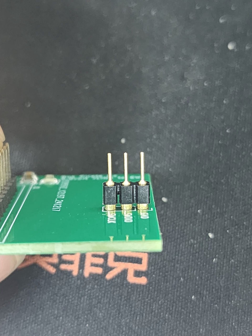
An issue I didn’t consider: the 3P milled pin header has about 3mm of stand-off from the board.
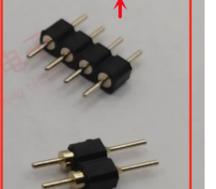
- Bottom type (what I have) has an additional metal stand under the plastic material
- Top type (on order) does not have the additional stand and is about 3mm tall. This is what we sourced for the board.
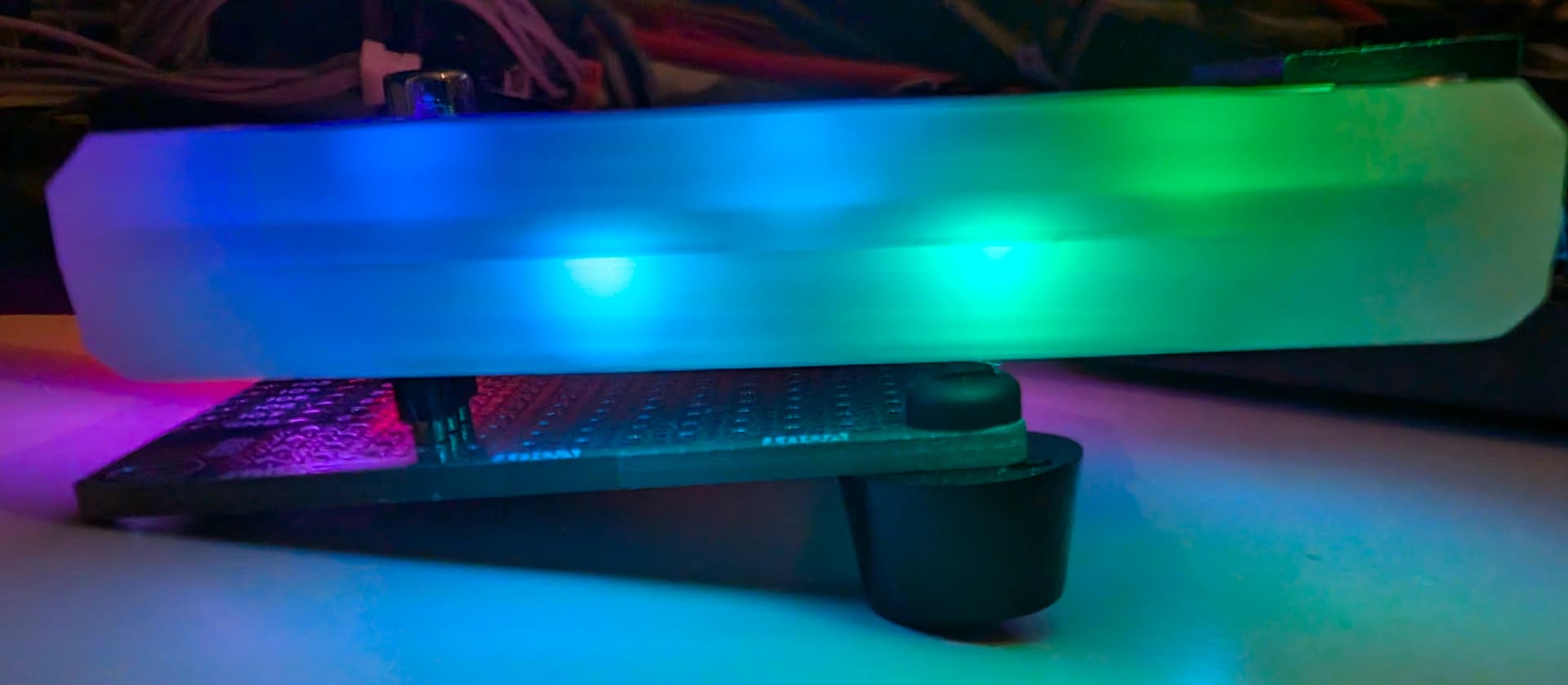
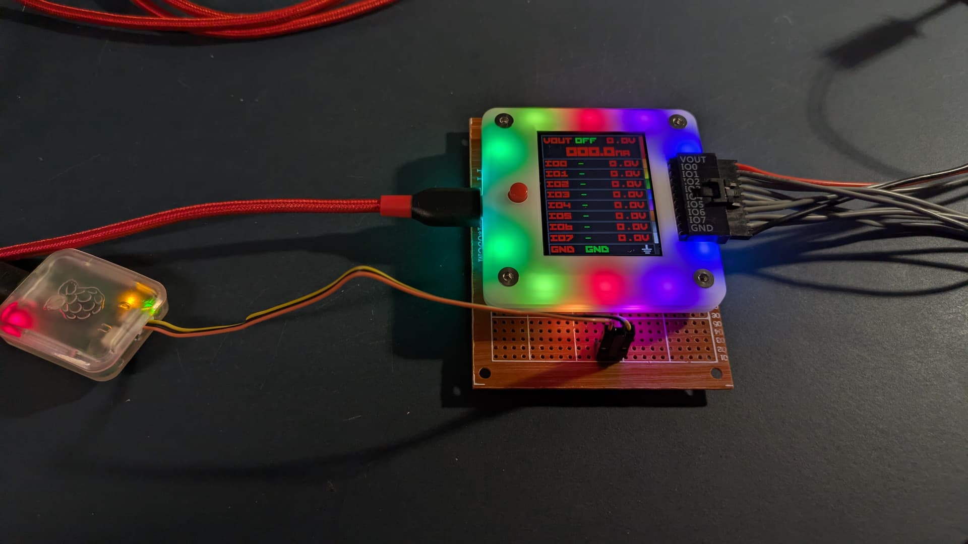
This is an example with the extra metal stands. I’m not sure what to do about this. It kind of circles back to needing a cradle and eventually changing the programming connector type.
The issue is that the BP now is not parallel to the adapter board below, right?
Would the contact be reliable if it were, or is the contact of these kind of milled pin headers not good enough in your testing?
Maybe a shim under the screw on the right side in your photo could offset the height of these standoffs on the connector and make the BP parallel again.
1 Like
This is to demonstrate that the bus pirate will not sit flat on the adapter PCB. The contacts I assume will wear faster but the connections should be okay for some K of insertions. I use a tiny PCB and do this all the time, but it’s not the most elegant solution.
I think for a debug and development setup it doesn’t need to look perfectly polished. Also it doesn’t really matter if you have to replace the connectors every few thousand insertions. If you do that much plugging and unplugging, then you are developing heavily, so investing a few cents and minutes to solder on new connectors isn’t that much of an issue.
But you want it to always make a reliable connection when the connectors are not yet worn out. Because connection issues can be a huge time waste - you suspect some issue in the code, debug back and forth, scratch your head while reviewing the code and after many hours you find out it was just an unreliable connector.
1 Like
Maybe not the right place to post this, but…
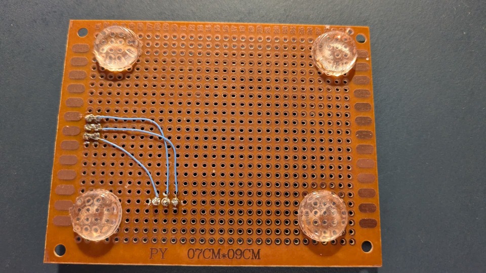
I decided to do a little light soldering this afternoon and make a more stable RTT adapter for the BP5 and Picoprobe.
I had a stack of small perfboard around. I soldered 3 of the milled breadboard pins into it. Then I soldered a 3x2 header on it (I only had two row header laying around, lol). Soldered some bodge/wirewrap wire between the milled pins and the header. Added some rubber feet to the bottom of the whole thing to keep it in place on my desk.
Once I put the BP on the top, I realized I had the same stability kind of problem and tried putting 3 of the rubber feet on the top side. Success! It’s not pretty, but it works well and is stable ![]()
Of course it’s a lot more simple with a picoprobe.
4 Likes
Have had connection problems twice in the last year and a half that turned out to be frayed wires I soldered that didn’t have temperature proof coating. I only use silicone coated wire now.
3 Likes
I see a V2 case! That’s the one I think we should go with. Glad it arrived.
3 Likes
The case is really nice ![]()
3 Likes
OK, so we just need to add 3mm of EVA foam, or other slightly compressible support, to avoid stress on the connector. That is doable.
For next Gen BP, consider the debug port having an insertion motion parallel to the insertion motion of the USB-C connection. This would greatly simplify creating a dock with debug port.
3 Likes
BTW, for the style on the bottom … I think the larger diameter metal part is not supposed to sit on top of the PCB, but rather is intended to be embedded in the PCB. See also the counterpart:
I’m just guessing, but maybe that thicker post provides a stronger solder joint, and thus allows it to take more stress? In other words, I would guess that the slightly conical side of the male pins is the mating side, and the thick posts need a larger plated through hole for proper attachment? (then again, I’m just guessing … anyone know for certain?)
1 Like
@jin was also curious and asked the factory the difference between with and without the “step” and they said they don’t know ![]() It’s all just standardized tooling that factories buy in because that’s what already exists in the market.
It’s all just standardized tooling that factories buy in because that’s what already exists in the market.
Yesterday when we discussed this part I thought it might be interesting to do a very occasional video documentary digging into the history and basis for a single part. What standards are common in milled and stamped header and why? Why do all the SOT23-5 LDO vregs have similar pinouts and what is the origin. Sort of sourcing archeology .
2 Likes
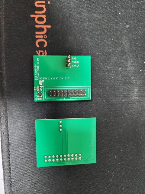
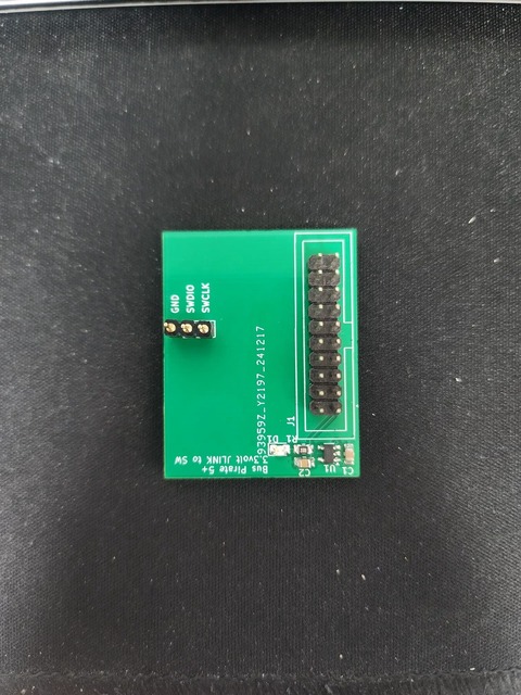
3 JLink adapter board prototypes are done. We sent (or will send tomorrow) one to @henrygab and @kd7eir. After we confirm it works, and the correct direction of the IDC connector, we’ll do a final version in a slightly larger batch.
3 Likes
Very nice! I like this idea
1 Like
Got a wonderful package today. Inside was the prototype board.
Board layout was fine
As can be seen, the orientation of the 20-pin header is correct. The key on the cable’s connector is facing AWAY from the buspirate. So, with a shroud, the slot would also be on the side furthest from the three debug pins. This is all as expected.
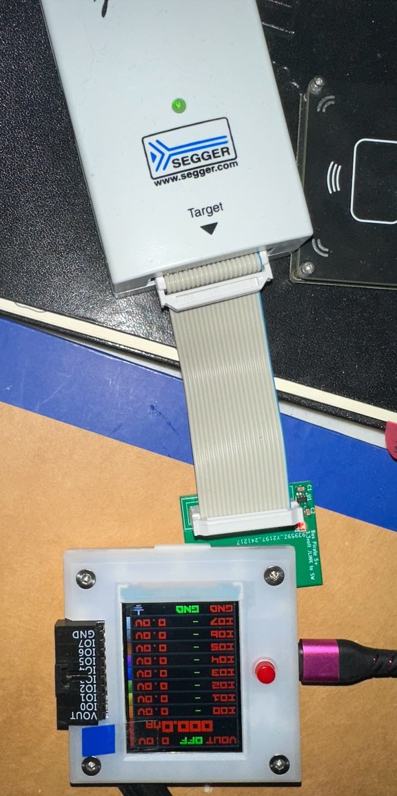
Connected and found the device
SEGGER J-Link Commander V8.10f (Compiled Nov  6 2024 16:15:11)
DLL version V8.10f, compiled Nov  6 2024 16:12:18

Connecting to J-Link via USB...O.K.
Firmware: J-Link V10 compiled Jan 30 2023 11:28:07
Hardware version: V10.10
J-Link uptime (since boot): N/A (Not supported by this model)
S/N: *********
License(s): FlashBP, GDB
OEM: ******
VTref=3.300V (fixed)


Type "connect" to establish a target connection, '?' for help
J-Link>connect
Please specify device / core. <Default>: RP2040_M0_0
Type '?' for selection dialog
Device>
Please specify target interface:
  J) JTAG (Default)
  S) SWD
  T) cJTAG
TIF>S
Specify target interface speed [kHz]. <Default>: 4000 kHz
Speed>
Device "RP2040_M0_0" selected.


Connecting to target via SWD
ConfigTargetSettings() start
J-Link script: ConfigTargetSettings()
ConfigTargetSettings() end - Took 213us
Found SW-DP with ID 0x0BC12477
DPIDR: 0x0BC12477
CoreSight SoC-400 or earlier
Scanning AP map to find all available APs
AP[1]: Stopped AP scan as end of AP map has been reached
AP[0]: AHB-AP (IDR: 0x04770031, ADDR: 0x00000000)
Iterating through AP map to find AHB-AP to use
AP[0]: Core found
AP[0]: AHB-AP ROM base: 0xE00FF000
CPUID register: 0x410CC601. Implementer code: 0x41 (ARM)
Found Cortex-M0 r0p1, Little endian.
FPUnit: 4 code (BP) slots and 0 literal slots
CoreSight components:
ROMTbl[0] @ E00FF000
[0][0]: E000E000 CID B105E00D PID 000BB008 SCS
[0][1]: E0001000 CID B105E00D PID 000BB00A DWT
[0][2]: E0002000 CID B105E00D PID 000BB00B FPB
Memory zones:
  Zone: "Default" Description: Default access mode
Cortex-M0 identified.
J-Link>
Other thoughts
Not recommended for use on flat surface without more. The edge of the buspirate with the USB port in my case was ~7mm off the flat surface. This put stress on the debug pins (and one bent). The pins having those large metal standoffs raised the height of the BP5. Definitely needs support.
I expect I’ll layer a few pieces of EVA foam, with cutouts for the PCB which will both lift the buspirate, and give me something to cut holes in when the new cases arrive so the feet don’t impact this. so that the buspirate can have a stable surface to rest on. Maybe I’ll even add some corner cutouts / guides in EVA foam, to make it trivial to align.
Recommended revisions:
- Shrouded, keyed header; key slot on side furthest from debug pins (yes, I know it’s already plan-of-record)
- Can the final PCB have an oversized hole for the foot of the new case’s to rest in? This will help a single “holder” support both the old and new cases.
- Fit’n’Finish … it’s a small thing … Can the corners of the PCB have rounded edges? Sharp corners are fine for the prototype, but even a few mm rounding would greatly improve.
- Luxury … So much PCB just begging for nice silkscreen art. Maybe the BP logo guy on the bottom?
Thanks for this! I will play around with some foam + manual cuts + rubber cement, see if I come up with anything reasonable as a “drop in” alignment helper / support structure.
3 Likes