DDR4 and DDR5 parameter table reader

@WiFiLuke started a thread about the i2c config chips in optical LAN modules.

It reminded me that Matt at Blinkinlabs suggested a DDR4 and DDR5 parameter tables reader and writer. It’s a similar situation with an I2C eeprom containing id info.

One, not sure which, needs a 9 volt supply which we can do with the SMPS plank.

I bought a weird breakout/testing board that covers 5 flavors and sizes of DDR to play with.

Blinkinlabs (one of our distributors) pointed me to a Arduino project for reading and writing SDRAMM/DDR2/DDR3/DDR4/DDR5 PC RAM parameter tables. The excerpts here are GPL 3.0 licensed.

All kinds of PC RAM since SDRAM have an I2C EEPROM that stores various info about the RAM stick and control version factors.

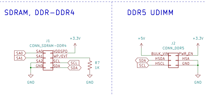
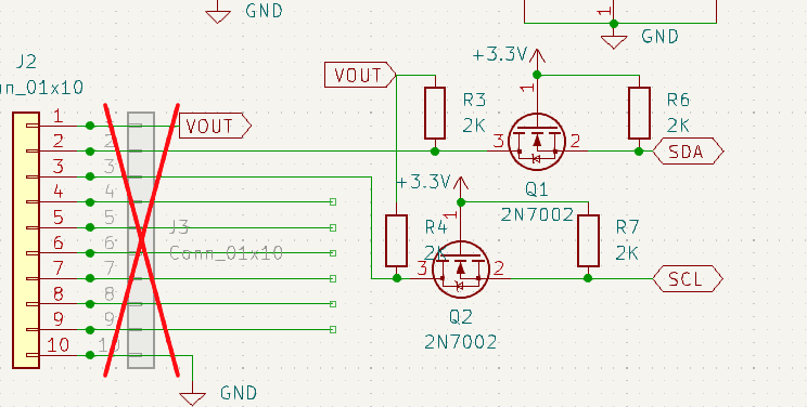
SDRAMM/DDR2/DDR3/DDR4 require a 9 volt programming voltage to make changes (SA0). SA1 is another 3.3volt control signal (WP?). SCL and SDA are the standard 3.3volt I2C clock and data pins.

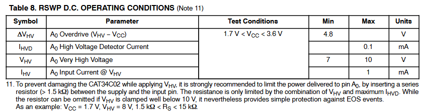
Onsemi CAT34C02 is an example of a DDR2 EEPROM chip. We can see here in the datasheet the Vhv is 7 to 10 volts to do certain stuff (write protect, unlock, stuff like that, let’s not get into details).

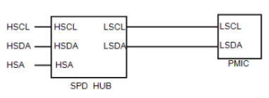
DDR5 is different in an interesting way. The EEPROM is now part of the “Serial Presence Detect hub” or SPD hub.

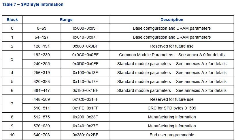
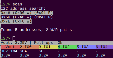
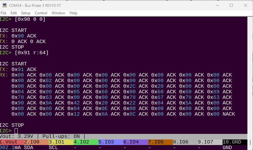
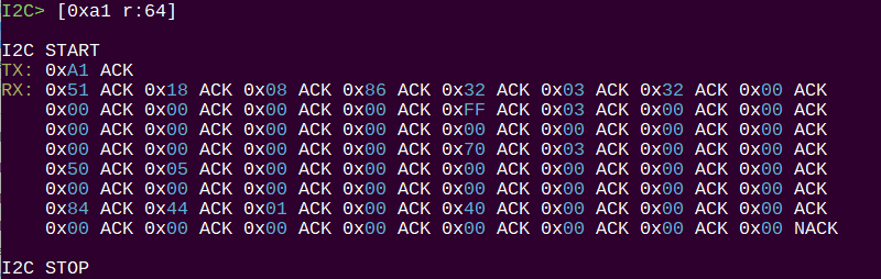
Here is the EEPROM memory map for an off brand DDR5 RAM.

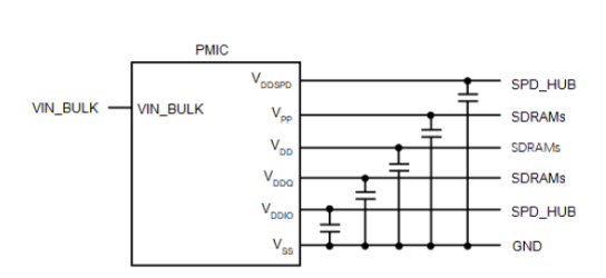
The SPD hub in turn controls a Power Management IC (PMIC). This chip takes a single 5volt supply from a single pin on the RAM module and outputs all the voltages needed by the RAM chips. This eliminates the need for an ever increasing number of voltage pins on the module, and frees pins for new features. Smart!


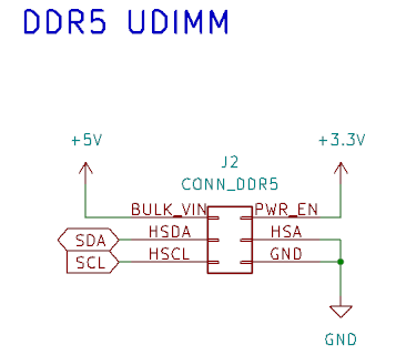
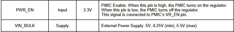
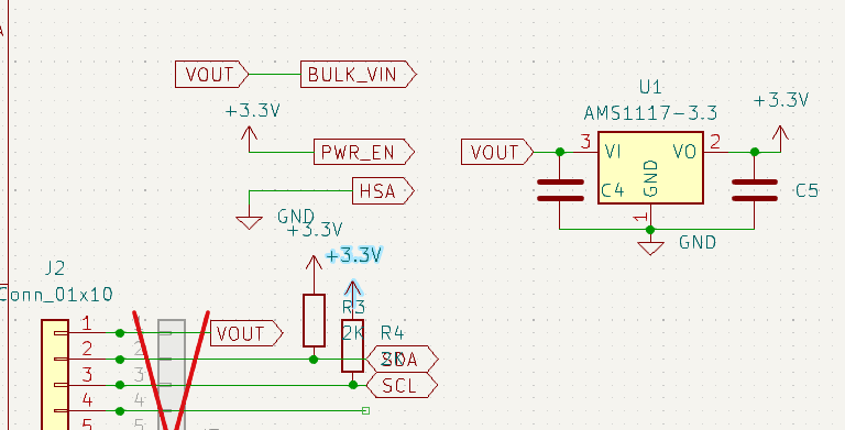
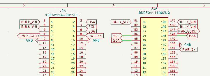
Looking at that DDR5 example from the Arduino project again, and we see the BLUK_IN pin. This is not a programming voltage like previous generations used 9V, instead it is a single supply that is regulated by the PMIC to power the module.

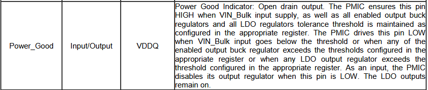
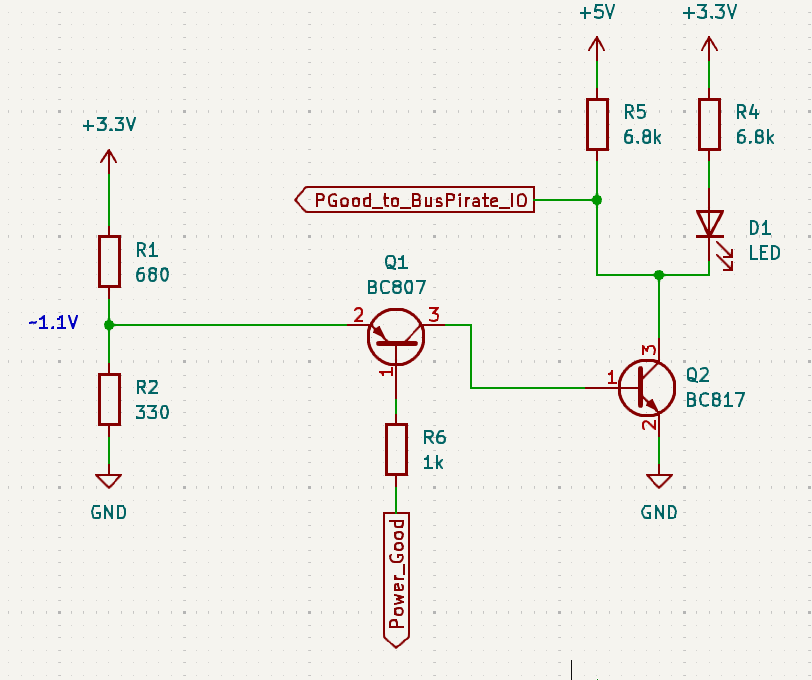
PWR_EN controls the PMIC, high/3.3volts to enable.

image

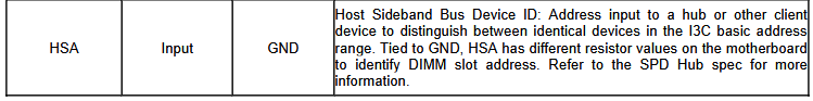
HSA sets the module I2C address, so a computer motherboard can tell the modules apart.

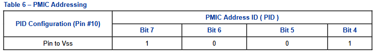
Each DIMM slot on a motherboard has a different resistor value attached between this pin and ground. It sets the I2C address according to some spec we don’t need to get into. In the Arduino project it is just tied to ground.

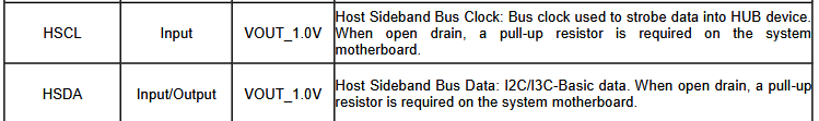
SDA and SCL are still there, though the chip can be elevated from I2C to an I3C mode. I’m not sure about the 1.0 volt note there.

Taking it further

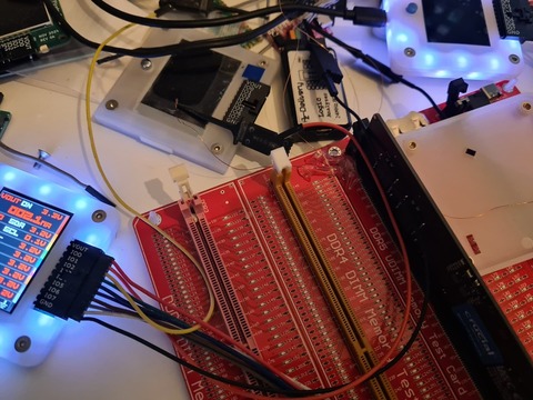
Starting with DDR5 because it is current and it might actually be useful for overclocking modern rigs. Also because we don’t need to deal with the 9 volt programming voltage. An ewaste stick of DDR5 RAM should arrive shortly. I bought a DDR3-5 tester board with nice sockets, but GRRRRR it doesn’t break out any of the needed IO pins.

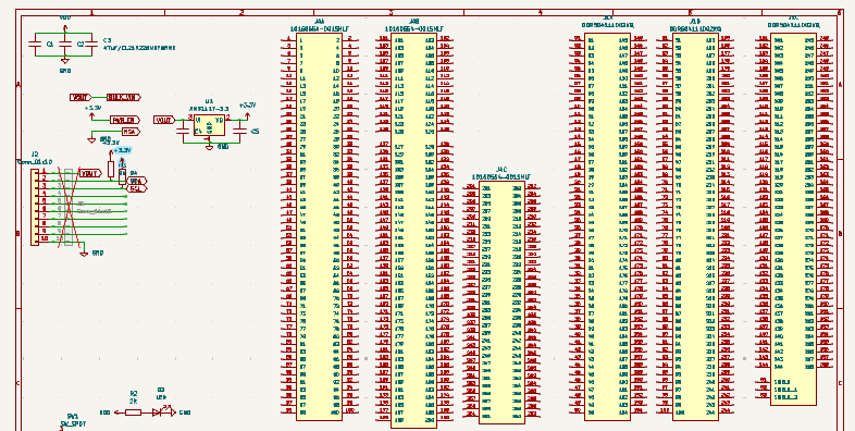
Quick mock up of a DDR5 UDIMM and SODIMM plank. Those sockets are huge and $$$.

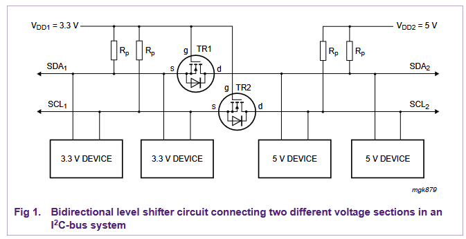
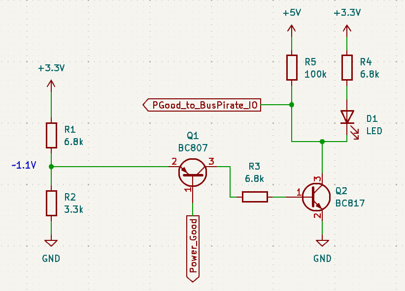
The IO needs a 3.3volt supply, but the bulk_vin needs 5 volts. My initial thought is to use the Bus Pirate VOUT at 5 volts. A regulator on the board provides 3.3volt for the control signals and I2C pull-up resistors. This isn’t ideal, as a wrong voltage on the I2C pin could break a module, so maybe some kind of simple bidirectional level shifter or a protection zener (yucky, probably). On the other hand the Arduino project above is running at 5volts and relies on the pins to stay open drain :slight_smile:

Resources

3 Likes

Bidirectional I2C level shifter app note:

2 Likes

I2C level shifting with two mosfets as shown in the appnote works fine in my experience. You don’t need any fancy dedicated TI parts for this unless you need extreme speeds or some uncommon 1.2V I2C voltages. So the 3.3V voltage regulator + I2C level shifter would be my recommendation. The 2N7002 as already used on the BP should work as mosfets for this.

I’m interested in playing with DDR5 UDIMMs and SODIMMs, as I’ve got some ECC RAMs that I would like to get working on desktop systems that currently still refuse to boot with them. Modifying the SPD would help to get further details about the exact reason. So I’m interested in this plank.

1 Like

Nice, this is the feedback I was hoping for. Everything works well enough for me that I’m not a PC tweaker anymore, but it seems to be a basic thing some people need.

I also read about some systems (Fujitsu?) That won’t accept generic ram modules because they lack a specific key in the spare bits of the eeprom. That seems like a good use case too.

1 Like

Yeah. I don’t know if my issues with the ECC ram come from not being from the right vendor or them being ECC. So copying vendor info would be one thing I’d like to try. The AMD processor should be able to cope with it.

2 Likes

Added the 2N7002 level shifter, along with some “courtesy” resistors on the VOUT side.

Next I’m going to probe my UDIMM breakout to see how it is wired up, then when the RAM stick arrives I’ll try to read the EEPROM.

2 Likes

Connected the needed pins on UDIMM and SODIMM sockets.

I haven’t actually thought about this, it is a note to think about it later :slight_smile:

Might be nice to have an LED light when power good is low. It seems like an open drain error signal that can be shared by multiple modules. However, VDDQ is 1.1volt, so I’m drawing a blank on how to turn off a PFET without an external 1.1volt supply for a pull-up. Even then, the Vgth (on our common PFETs) wouldn’t be enough to turn off the PFET with a 3.3volt LED. Maybe a PNP transistor is a better option, assuming the pin can take the current (which is unlisted).

2 Likes

I must prepend that I have never done any development with newer ram standards like DDR4 and 5, and especially in DIMM form. So take my comments with caution.

The signal is called “Power_Good”. This is what is in the DDR standards, this is what people will read up if they are interested in it for some reason. So why negate it? Why not use a positive Power_Good LED that lights up green when everything is ok? I think this will give the least possibility of confusion for the users.

The 1.1 V VDDQ is created by the PMIC on the ram module, correct?

I suggest to use the Power_Good signal to drive a common NPN transistor with something like 10k as a base resistor. So current will flow through the NPN when Power_Good is high.

This will load the Power_Good pin just in the µA range and I’m pretty sure that this is something the RAM modules can drive without issues. And a NPN that is driven with a 10k base resistor will easily be able to drive a common LED current of something like 1 to 5 mA.

We could also hook up the collector of the NPN to an IO of the BusPirate so that we can read the state of Power_Good. Add something like a 100k pullup so that the logic signal isn’t confused by the LED in parallel.

2 Likes

It appears to be open drain though. Input or ground.

2 Likes

Hmpf. I know why I put that warning in front of my post :face_exhaling:

I guess I’ll better draw a small schematics to not get confused again.

2 Likes

I think a PNP will be OK, but without real specs I don’t know. In this instance we could fry someone’s 48gb killer ultra predator cool RGB with heat spreaders whatever ram stick. It gives me pause, at the expense of an extra led.

The €15 ewaste DDR5 arrived from the recycle shop. I thought it would be no name, but it is a proper crucial stick with nice timing, still in the proper clam shell case.

2 Likes

What do you think about this circuit:

The current drawn through the Power_Good signal would be about 400µA max. and will never be higher than 1.1V due to the voltage divider. I am pretty sure that 400µA won’t overdrive the PMIC on the DIMM. I wouldn’t want to push in 10mA, but µA aren’t an issue with logic outputs that are designed to cross over to another PCB.

Edit: I think 6.8k for the pullup to the BusPirate-IO would also work, and would reduce the BOM.
With the two transistors in series we don’t need to worry about not having enough current drive capability.

And we need two transistors, because with just about 1.1V you can’t properly drive an LED. Maybe an IR one, but being invisible would defeat the purpose.

2 Likes

Bah. Don’t trust what I’m doing tonight. The Power_Good would eat all the current and would not leave enough for Q2 to open.

This should be better:

2 Likes

Searching Taobao for 连接器插座内存槽 seems to turn up a bunch that are affordable (but the pcb will be huge of course).

2 Likes

Thank you for the indicator circuit, it looks good. I was having trouble getting my head around doing it with FETs, PNP/NPN is definitely the way to go. Will add this.

Made this mess. 5volts from one Bus Pirate, 3.3volts + I2C from a second.

Pro tip: don’t setup the giant & delicate mess where your keyboard normally sits…

We found I2C addresses!

The first appears to be an EEPROM with not a lot of info in it. [0x90 0 0] to reset the read pointer, [0x91 r] to read. If the read pointer is not reset it does not start from the beginning of the EEPROM array, eventually it loops around.

The second address does not appear to be an EEPROM. The same data reads out without resetting the read pointer. I suspect this is the PMIC or a second address on the SPD for interacting with some kind of voltage and temperature monitor.

Second to last line 0x84 0x44 toggles between 0x40 and 0x44 when I warm it up a bit. Suspect this is a temperature monitor.

Thanks! Will do this and finish up the schematic now.

1 Like

Indicator LEDs.

Next I’ll choose a socket and send the board for routing.

2 Likes

did you get a few bugs inserted due to nudging stuff around?

2 Likes

No, but I had to use my keyboard awkwardly on the far corner of my work table.

1 Like

This one probably shouldn’t plug directly into the Bus Pirate… Perhaps a 5 pin header that attaches to the probe cable?

It looks like LOTES and Foxconn make lower cost DDR5 sockets that follow the Amphenol “standard”. Still looking for a proper drawing to confirm it’s a match.

4 Likes