Thank you so much, that may help. I’ll see if I can find that in the spec and expose it in the ddr5 command.
2 Likes
I checked the SPD datasheet, and didn’t see any volatile settings that lock the voltage or not.
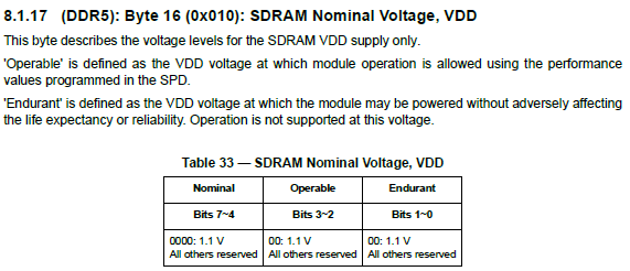
I read through JESD400 about the volatile area of the SPD. Bytes 16, 17 and 18 seems to set various voltages, but the only option is 1.1 volts.
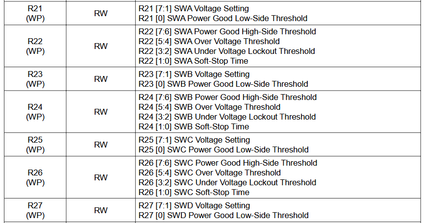
From the richtek datasheet for the PMIC, we can find the R21/25/27/1d/23/24 settings mentioned in the chart.
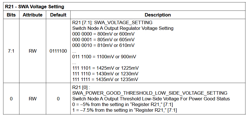
Closer look at R21.
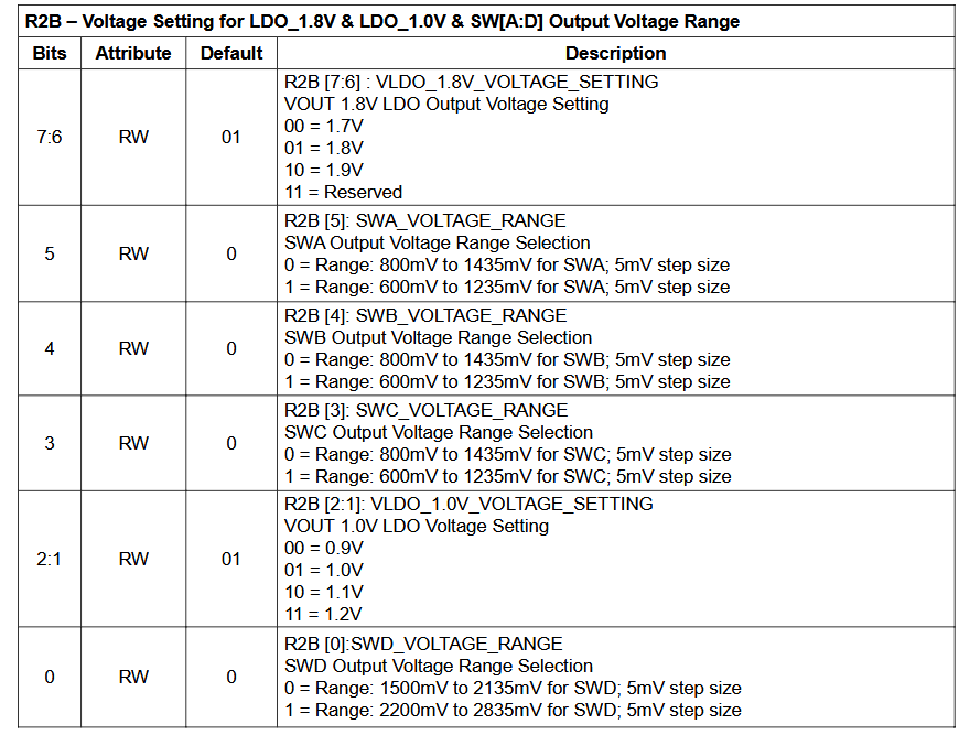
R2B which seems to have something to do with control.
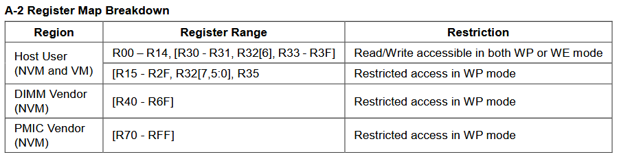
Those registers are only accessible in WP mode. What is WP mode?
Note: R15 to R2F, R32 registers are read-only in write protection mode as CAMP signal is at logic high level. Denoted
“WP” in “Register” column for clarification
So access to Write Protect is write protected? Must be a signal from SPD to PMIC or is also uses the same offline mode indicator as the SPD.
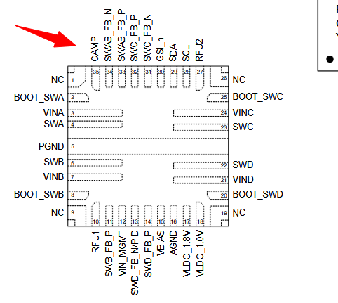
I see the CAMP pin on the chip.

This might be something similar, it disables the function of the CAMP pin.
So what I kind of understand at this point:
- You have a DDR5 that has some kind of lock bit programmed in presumably the PMIC that prevents overclocking/voltage customization
- The lock bit and the voltage control bits are protected by the status of the CAMP pin. We currently do not know if CAMP is the same as offline mode or if it is controlled by the SPD itself.
- None of these bits are marked ‘E’ for non-volatile (persist after power cycle). I could have missed something, but I’m not sure the settings will even stick after power down.
My limitation here is that I know very little about the PMIC and even less about how the PMIC actually connects to the SPD.
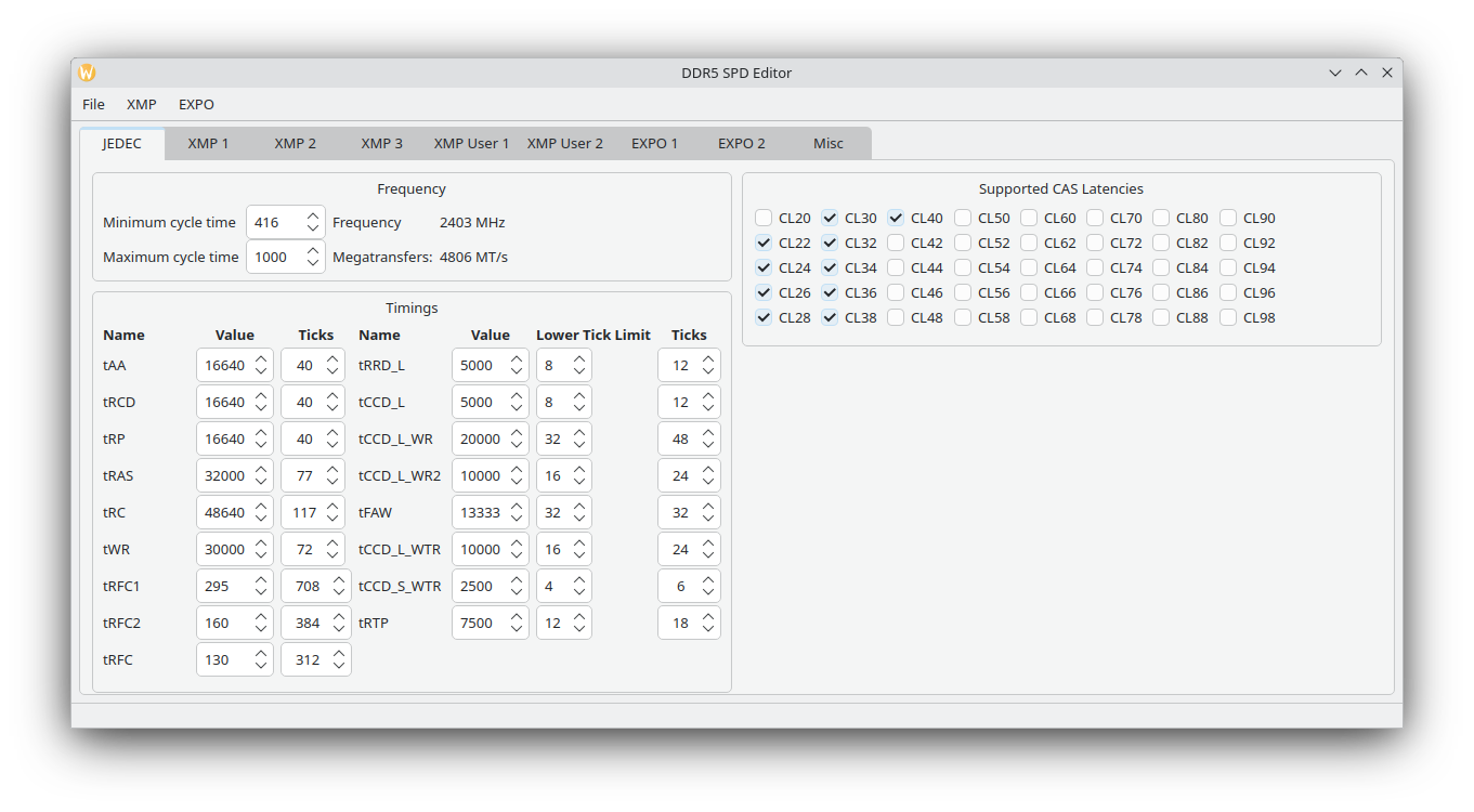
This DDR5 SPD editor doesn’t allow voltage changes in the JEDEC profile, so that’s consistent with what we saw earlier.

It does allow to craft custom XMP and EXPO profiles with custom voltages.
However, if the PMIC itself is preventing voltage changes, then I’m not sure the settings in XMP or EXPO profiles will even be accepted.
If we can get a clearer understanding of how exactly the PMIC is being locked, I can probably write code to manipulate it.
Warning, slop
Based on the JEDEC DDR5 PMIC spec (PMIC5010, e.g. Richtek RTQ5119A), the lock you’re hitting is Write Protect mode.
The lock bit
- Register 0x2F bit [2] — “Write Protect Function Control”
0= write protect is enabled (default; controlled by CAMP pin)1= write protect is disabled (all registers always writable — lab/debug only)
While write-protected, the PMIC ignores writes to the host configuration region R15–R2F and R32, plus the DIMM vendor region R40–R6F. That range is exactly where the SWA/SWB/SWC/SWD voltage setting registers live (R21, R23, R25, R27), so voltage changes are blocked. Reads are still allowed.
How CAMP gates it
CAMP (Control AND Monitor Port) has three roles; one of them is the write-protect input:
- CAMP input HIGH → PMIC enters write-protect / “Online” state → voltage registers locked
- CAMP input LOW → PMIC enters “Configuration” state → voltage registers writable
CAMP is open-drain with an external pull-up (typ. 10 kΩ to 1.8 V on a DIMM). On a normally-running DIMM the host lets it float high, which is exactly why the part is locked during normal operation.
How to unlock to change voltage
Three legitimate ways the PMIC will exit write-protect mode:
- Drive CAMP low externally (host or test fixture pulls it down). This is the intended path.
- Power cycle VIN_BULK and VIN_MGMT simultaneously.
- Internal fault (VIN_BULK OV/UV, SWx OV/UV) — PMIC asserts CAMP low itself.
Lab-only shortcut: set R2F[2] = 1 to disable write protect entirely. The datasheet explicitly warns this is for lab/debug, not normal system operation.
Important CAMP side effect: Fail_n
CAMP doing High→Low has a second function: Fail_n. By default (R32[4] = 0), a CAMP high-to-low transition also issues a VR Disable — i.e. it powers the rails down via the power-off sequence and clears R32[7]. So if you just yank CAMP low to unlock, you’ll typically lose the rails too.
To change voltage on a live system without dropping the rails, you must disable Fail_n first:
- Set
R32[4] = 1(Fail_n disabled — CAMP low no longer triggers VR Disable). - Drive CAMP low → enters Configuration mode, registers writable, rails stay up.
- Write the new voltage to R21 / R23 / R25 / R27 (and matching OV/UV thresholds in R22/R24/R26/R28 if needed).
- Release CAMP back high to re-enter Online (write-protect) mode.
Note also R32[3] (CAMP PWR_GOOD output control) and R32[5] (Execute VR Enable) — relevant if your platform’s CAMP line is being driven low by the PMIC itself due to a latched fault. In that case you must first clear the underlying status and then the host can release CAMP.
TL;DR
The lock is Write Protect mode, gated by the CAMP pin and configurable via R2F[2]. Unlock = pull CAMP low (or set R2F[2]=1). To do it without killing the rails, set R32[4]=1 (disable Fail_n) before pulling CAMP low.
For what it’s work, Claude slop overview of the datasheet basically says put CAMP in write mode, but the rest of the advise is slop because we can’t write any of the mentioned override registers while in WP mode.
For good measure I checked the DDR5 & SPD datasheet and CAMP does not seem to be an exposed signal.
There is some mention of being unlocked before the DDR5 is online, so maybe it’s as simple as bringing it up on the plank in offline mode and then writing the bits. However I did not dig that deep into the datasheet and suspect that is just slop.
1 Like
Sorry for the late reply and thanks for doing some digging!
I had been digging through this a bit, both the jedec pmic5100 doc and whatever pmic/spd datasheets I can find.
As you found out, nothing on the PMIC specifically would “lock” or write to 0x2F. The dimm vendor startup configuration registers don’t seem to include a configuration for this nor is 0x2F copied from the dimm vendor region to the host region (as some others are).
Yeah, the datasheets I could find didn’t make a single mention of the CAMP pin at all. They all seem to indicate that the 0x2F needs to be set to programming mode by the host before VR_ENABLE signal is sent and that’s it.
What hurts my brain about that is there must be something going on spd/pmic side that locks that out (maybe the camp thing?) as there are both dimms/sodimms that come from the factory being able to be “unlocked”, so it’s not as though the host motherboard isn’t trying to set 0x2F appropriately.
As far as I can tell, the “CAMP” pin is being referred to as “PWR_GOOD” in the PMIC docs. GSI_n is also mentioned a lot with them as well. I wouldn’t be surprised if those two plus masking bits play some role in how the PMIC is being forced into “secure mode” by some programming, somewhere. (I just saw you already made the connection in your own docs haha).
I looked through the spd writer code as well and funny enough, they recently tried to allow jedec voltage changes but reverted the change as it didn’t seem to work. I don’t know how they tried to edit jedec voltages (probably something worth asking) but I do not think merely adding them to the jedec timing registers (as is done with xmp) is enough.
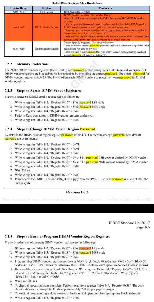
One possible avenue would be to alter the dimm vendor region registers for voltages/thresholds (yes, would be a pain from an ‘in the field’ perspective but ..). During the power up sequence, the dimm vendor region registers are copied over to the internal PMIC registers.
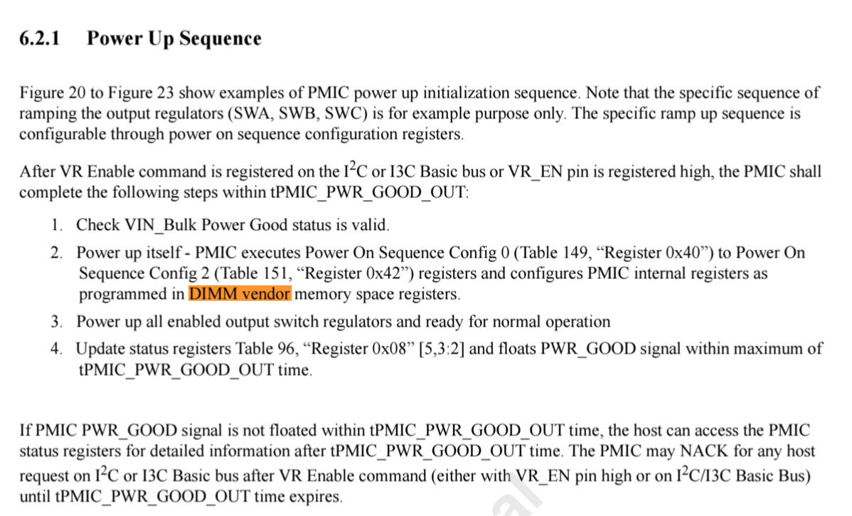
There is a default password for the dimm vendor region. From experience of other ICs, most will leave this password at default: “The default password for DIMM vendor register is 0x9473.”
As for the write protected stuff, it seems you are looking at PMIC5010 documentation. From my findings, most consumer level dimm/sodimm are using PMIC5100 standards (and the PNs on the dimms I have looked at all come back as such). This may be why I don’t see any reference to ‘CAMP’ (I have been using jedec PMIC5100 docs). It seems the method for disabling WP is much more straightforward on consumer dimms (from what I can see).
This still doesn’t change the fact that something is preventing host changes in programmable mode.
I am adding another photo (can’t add two since I’m a new user) below for the process of accessing/writing to dimm vendor region.
I didn’t add much to the conversation but thanks again for taking a look into it.
1 Like
Dimm vendor writing process:
I have also stumbled upon this fun project:
https://github.com/H43TO/Unified-DDR-Flasher
Which seems to have pretty good knowledge of PMIC programming
1 Like
Just a guess, but perhaps the manufacturer can choose to tie CAMP high/low to enable/disable any voltage changes? In this case they locked it but modules that support extended profiles leave it unlocked?
I’d really love to know the answer if anyone finds it 
1 Like
I asked on the GitHub I linked if they have attempted as such with their own equipment. We shall see if we can get some more insight into the matter.
2 Likes
As an update, the creator has replied and confirmed that the only way they could apply voltage changes is to overwrite the dimm Vendor region (on “locked” sodimms), so one of the avenues that was guessed here.
Now, whether this actually unlocks the ability to alter voltage from the host OR merely just sets a default voltage to whatever is written I don’t know, waiting for their response to such a question.
2 Likes
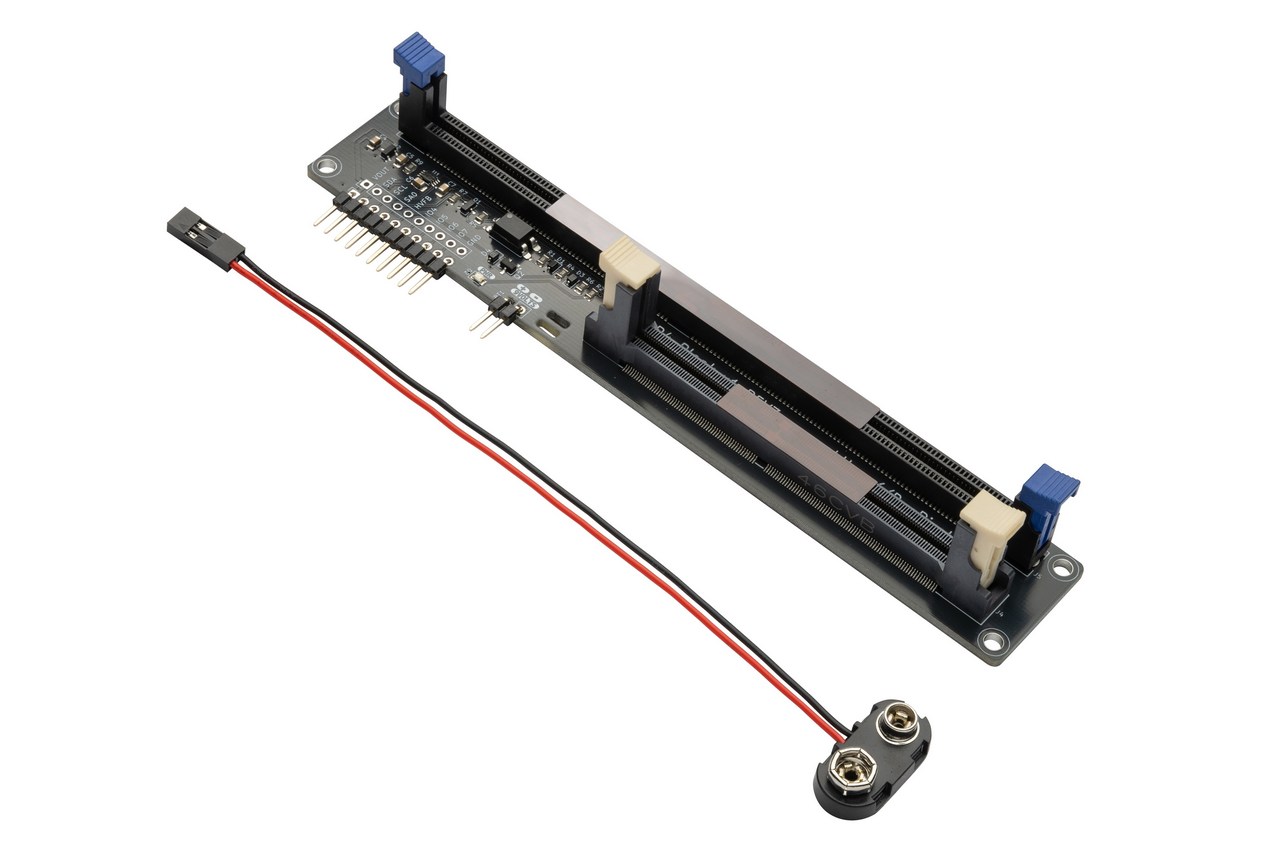
It took a while, but the DDR4 plank is now available.
Read, write, lock and unlock the I2C SPD chip on DDR4 memory modules with Bus Pirate 5+.
DDR4 adapter design, DDR4 command and low level SPD interfacing is covered in the Bus Pirate documentation.
- 288 pin DDR4 UDIMM socket for standard desktop memory modules
- 260 pin DDR4 SODIMM socket for laptop memory modules
- 3.3 volt to 5 volt power supply
- A 3.3 volt regulator ensures the DDR4 module VDD pin is never more than 3.3 volts
- A level shifter ensures the I2C pins SDA and SCL are never more than 3.3 volts
- SA1 and SA2 are pulled to ground to set the I2C address to 0x50
- SA0 is normally ground, an optocoupler can connect it to 9 volts to change the write protection settings
- External 9 volt power supply required (typically a 9 volt battery)
Sorry for the long lead time. The plank has been ready for months, but the photographer we use imploded and it took a while to find a suitable replacement.
The DDR4 adapter plank is ready to use, but you'll need a 9 volt battery or bench supply.
1 Like
Did you ever get anywhere with figuring this out? I suspect this is the exact issue I am up against with my Corsair sticks. My initial thought, before seeing what you have found regarding the lock, was to just alter the manufacturer part number to the version that is supported by the motherboard QVL. The kits are nearly the same on paper, but now it is making sense why mine is not on the QVL if the voltages are locked out. I am guessing it is punishment by Corsair for the cheaper kit to locked and restricted 1.1V vs. their more expensive flagship kit, with the exact same components, yet unlocked to alter voltages and overclock your heart out.
1 Like
Evil. They’re onto our software tricks and are doing it in hardware where you need a bit more skill to override it.
One of the Xbox (?) Hacks was drilling a certain part of the main chip to disable a die that locked it down. Maybe there’s a similar pathway here?
Hey so yes I did. That GitHub moved, for whatever reason, to here: https://g.i.t.h.u.b.com/H43TO/Unified-DDR-SPD-Flasher
(Remove the dots from GitHub. Won’t let me post it otherwise for some reason)
I had asked them about it and this was their response:
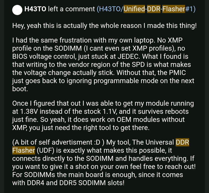
So was one of the avenues guessed above. Basically, you have to completely flash over the vendor locked region (which is limited to, I think, 3 flashes before being fully locked/dead) with the voltage you want to use. This can be done for vdd, vddq and vddp, which each have their own registers.
I had asked if this would allow manual voltage control in bios afterwards but didn’t get a response. I haven’t looked at the docs recently but I would surmise it should be possible IF the vendor region contains that a byte (I listed it above but it’s in the consumer pmic doc I listed as well).
The PMIC5100 doc is what you want to look at for all of this if you want to understand how this works. The password for that region is most likely going to be just the default (that GitHub lists it as well as the docs). The doc isn’t difficult to navigate but is large. That screenshot I posted above about the region writing (the one with the password) is what you will be focusing on.
But yeah, lump sum, you need to pick your voltage before flashing (and just use stock timings if your bios allows timing changes) and be confident that’s what you want to use. You only get 1 (maybe 2) more tries if you want to change it again.
I think i got your post restored. Thank you so much for the info.
1 Like
it was drilling on the drive chip to disconnect a bond wire
1 Like