Port protection for Rev7

Before talking parts and configurations, I’d prefer to take a step back and look at the goals of the port protection first. I thought a new thread makes sense for this.

So what is the regular usage that is required?

Vout:

  • 1-5 V output at about 400mA max

IO-Pins:

  • 1.2 to 5V digital IOs
  • A digital signal > programmed Vout, but < 5V should keep the BP input in high-impedance (no excessive current through diodes and such)
  • Should be able to drive old-school TTL (= 1.6 mA into fanout of 10 should keep the max drop < 2 V)
  • Input and Output of 25 MHz digital signals without distorting the waveform too much
  • Interface with parasitic power Onewire and similar (power through 1.something k pullup)
  • Interface with Fast mode plus I2C (20 mA pull-down required) (not realistic)
  • Active analog measurements in combination with the new pulls (Port impedance measurement, Component tester)
  • High Impedance Analog Voltage Measurement: Protection diodes should not have too high leakage

Abuse to protect from

Vout:

  • ESD
  • Short overvoltage pulses (pos and neg), like when powering a relay without freewheel-diode
  • Back-powering to a higher voltage than selected
  • Back-powering when BP powered off
  • Connecting a negative voltage
  • Connecting a negative voltage when BP powered off

IO-Pins:

  • ESD
  • Short overvoltage pulses (pos and neg), like when directly driving a small speaker with PWM and no freewheel-diodes
  • Connecting a higher impedance negative DC voltage, like RS232
  • Connecting a higher impedance positive DC voltage >5V, like 4-20 mA @24V
  • Connecting a low impedance negative DC voltage, like a power supply
  • Connecting a low impedance positive DC voltage >5V, like a power supply
  • all also when BP powered off
  • Also when an IO port is configured as output (-> back-powering)
  • Killing a connected DUT by shorting digital IOs
  • Killing a connected DUT by accidently using a higher voltage than allowed

When connecting a power supply it would be nice being able to survive 12V,
since this is a quite common voltage. 24V would be cool, but probably not
realistic without compromising the other goals or increasing cost & board space
too much.

The goal of not killing a DUT with too high voltage is difficult, because the
integrated protection diodes often won’t allow more than like 10 mA before
being damaged. But even more current is required for the FM+ I2C and TTL to properly work, so we have conflicing goals.

Does this list look good? Something missing, wrong or too ambitious?

There are probably more conflicting goals than the DUT-killing here, but I prefer to explicitly spell them out and discuss them.

2 Likes

That’s a good wish list. 12volt tolerance on VOUT is something I haven’t considered.

I tend to think about what I need to protect:

  • DUT (don’t burn out pins while making mistakes learning a new device)
  • 74lcv1t45 IO buffer (these are pretty robust and support partial power down, so they don’t allow back powering, maybe more robust ESD protection?)
  • The analog measurement bits (currently CD4067, but any future (SPI) ADCs: prevent back power, some robustness against over/under voltage spikes and ESD. Currently protected by current limiting resistor, diode to VUSB, and buffered with opamp. The primary goal being to prevent back powering)
  • The pull-x resistor system (currently PFETs and R array, will be a TCA6416 which I believe has partial power down Ioff feature)
  • 74lvc8t45 follow along logic analyzer buffer (This has the same robust partial power down Ioff features as the single bit buffers)
  • VOUT (has a one-way value to prevent higher voltages from entering the power supply)

One major short coming of the current IO pin setup is that the protection is entirely intended to prevent back powering through the analog measurement bits. A resistor limits current to what a schottky diode can sink to below +0.3v when back powered.

This may also have the benefit of protecting the opamp from positive voltage spikes, but is not the intention. When we have space I’d at minimum add a schottky diode to ground (there is a nice dual package).

Disclaimer: The information provided is not my work and I do not take credit for any contributions that come from the contents.
The information has been provided by a source that I do not have explicit permission to disclose their identity, so I am posting this to contribute to the knowledge base, as they don’t have an account or would prefer to not post here.
I would like to express my gratitude for their time and efforts to provide information for the project.

Reply Below:

"This is where things can get “interesting” and very much is where “pro” equipment differs from hobby. Somewhere in the middle however there are often compromises that can go a long way to dealing with all those nasty corner cases created by accidental and/or intentional misuse.

For purely digital inputs and outputs I tend to leverage transistors as a saturated switch, selecting the maximum voltage and current capabilities to align with the anticipated maximums.

For analog it becomes harder and that is where op-amps can help. For a lot of my ATE devices I have had great luck with the OPA547, OPA548, OPA549 and similar where I needed to supply an output voltage where I expected some degree of current draw, but things can get expensive quickly.

If it is ESD then there are a number of good devices available now https://www.ti.com/lit/sg/sszb130d/sszb130d.pdf?ts=1729478283358

Although much of this may be obvious this, may be helpful to some: https://community.element14.com/technologies/connector/b/blog/posts/5-things-you-need-to-know-about-i-o-port-protection

For power outputs I have often designed electronic fuses, but that may be overkill for this kind of product."

1 Like

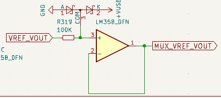
Protect opamps against negative voltage spikes

image

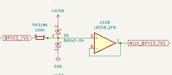
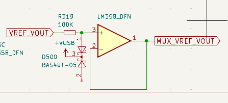
Currently a single BAS40T-05 works with a 100K resistor to prevent back powering.

image

For additional protection against negative voltage spikes, each opamp will now have a BAS40T-04 to VUSB and ground.

  • Confirmed: BAS40-04 in sot-523 is a standard production part, we can use it

TVS protection for pins (VOUT?)

Nexperia PESD5V0L1BSF bipolar TVS diodes look promising to me. I’d rather use a well characterized part, at least during prototyping. Then try some cheap parts later.

  • One on each IO pin
  • One on VOUT/VREF??

Continuous over voltage protection

I’m not sure how @electronic_eel envisioned 12v tolerance. One thing I could think of is a 5.6 or 6.2volt zener diode (tolerance is generally sloppy) on each pin and VOUT.

It seems like some kind of small value series resistor would be needed to keep from blowing out the zeners if they really were connected to a strong e.g. 12volt source.

2 Likes

Sorry for only replying now, it was quite a busy week for me.

I added the point “High Impedance Analog Voltage Measurement: Protection diodes should not have too high leakage” to my first post.

I’ve seen that you added TVS diodes to your current git revision 7-rev0a and lowered the series resistance to 120 Ohms.

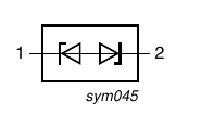
Currently you have DESD5Z5.0 TVS diodes in the schematics. These are bidirectional types, so essentially they are built out of two zener-type diodes back-to-back like this:
Screenshot_20241103_224734
This allows minimal capacitance, but this model isn’t really good at this (the Nexperia datasheet for these lists 12pF, CBI lists even 25pF). The biggest downside is that these diodes can’t protect against negative voltages lower than 5V. But the 74LVC1T45 just allow -0.5V. Also they have to dissipate all the overload energy alone.

So I suggest something different:

First put the TVS diode behind the resistor. This reduces the protection for the 74LVC1T45, but it means that the TVS diode doesn’t have to survive all fault energy alone, as the resistor will drop a substantial part of it.

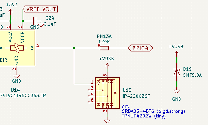
The other part is the design of the TVS diode. The parts I suggest are a combination of a series diode array and a zener. So they are connected to gnd and VUSB and if the input goes above/below the rails, these series diodes conduct first. The voltage is dumped into the power rails, which have e.g. capacitors to charge and so on, so there is somewhere for it to go. If this isn’t enough they also have a zener-part which can dissipate some of it. But since you are on the (one) power rail now, you can also support this by putting a little bigger TVS there, like the SMF5.0A I suggest.

These type of TVS diode arrays are common for example to protect USB ports. They are available in different sizes:

  • TPNUP4202W: SOT-363, 0.6pF capacitance
  • IP4220CZ6F: SOT-23-6, 1pF capacitance
  • SRDA05-4BTG: SO-8, 8pFcapacitance, 600W in a 80/20µs pulse

Now consider the case with the +12V on an IO-Port:

  • the protection won’t kick in exactly above 5V, but start at something like 6V. So you have 6V left to burn
  • 6V through 120 Ohms are 50 mA
  • 50 mA * about 1V forward voltage are 50 mW at the TVS-diode
  • 50 mA * 6V are 300 mW at the resistor

So in this scenario the TVS diode isn’t the limiting factor at all, but the 120 Ohms resistor.

The 0402x4 resistor arrays are usually rated 1/16W (62.5mW) at 70°C. At nearly 5 times overloading they will burn & die fast. You could put 3 times 39 Ohms in series or I suggest to go to individual thick film resistors in 0805 per channel instead. These offer 500mW at 70°C:

They will still heat up very much in this scenario, but won’t instantly be fried.

1 Like

When putting the TVS diode behind the resistor, you have to consider the low-pass filtering effect. This could affect higher frequency digital signals.

120 Ohms and 10pF (the input of the 74LVC1T45 also has some parasitic capacitance) still looks reasonable to me:
https://www.falstad.com/circuit/circuitjs.html?ctz=CQAgjCBMB0CsCmBaMAGELpjAZm2ALABz6zYoBs5hk524IsDaCyYAUAErgCckUKhcPnz9BaPpFgppMkNmh00SuGwBOPCQLkoRkLWjB62AY226tZEZfTgkWKNHIB2J9liEw5WLHwFuY6Gl2AHMzMOtcchsUNgAHML1BYUFEuWi2UOTRECzJKKU2AHsc+jR8FH8GdEwbdiA

But for example with 120 Ohms and 25pF I you might often still get away with it, but I don’t like it:
https://www.falstad.com/circuit/circuitjs.html?ctz=CQAgjCBMB0CsCmBaMAGELpjAZm2ALABz6zYoBs5hk524IsDaCyYAUAErgCckUKhcPnz9BaPpFgppMkNmh00SuGwBOPCQLkoRkLWjB62AY226tZEZfRQ4SLCEQZIZHSm7Yae7N3x8M0uwA5mah1rjkNihsAA6heoLCgglyUWwhSaIgmZKRSmwA9tn0aPjugowYEAZsQA

This is because the DUT will often have some similar input/output stage with a resistor of similar order of magnitude, and then there is the capacitance and crosstalk of the wires and so on.

So I think when using 120 Ohms and a TVS with single-digits pF it will work out.

1 Like

How well have you tested the back-powering-protection circuit you have on the BP5 and newer?

Would it work for example to protect the voltage regulator and 74LVC1T45 etc. from external 12V that you put into Vout?

What if you connect negative 12V there? This should create a high current and the current limiter should kick in, but this is most probably not enough to protect the voltage regulator as it is just rated for 6V. Maybe a second P-FET could be wired anti-series to the existing back-powering-protection one and used as reverse-polarity protection?

The opamp to sense Vref-out should survive due to the 100K resistor limiting the current.

1 Like

That’s a lot of great info to consider, thank you. Those parts do have MUCH lower capacitance, and the USB protection devices make total sense.

If the TVS diode is after the resistor, then it is only for the protection of the 74lvc1t45? Not for the opamps as well?

I imagine that if you put 12volts to VOUT lots of things would go poof. VOUT has a one way valve (up to 5volts as you note) protecting the power supply. Half the buffers, I2C expanders, fala buffer chips are all powered directly from VOUT and would I assume die. As would the one way value PFET.

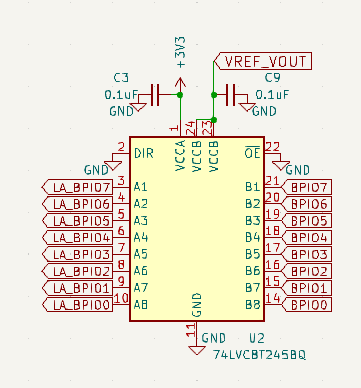
I read the datasheet for IP4220CZ6F and that seems like an ideal alternative, and we’d only need 2 (3 if on VOUT).

It will take me a bit to digest this info, I’ll be back with more.

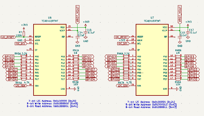
It is only for the 74lvc1t45 and the gpio-extenders for the pulls. So the gpio-extenders for the pulls should also be connected behind the 120 ohms resistors to get under their protection mantle.

The opamps currently have a 100k resistor in front and an extra BAS70 series diode in front of them. Opamps are usually specced to allow ±10mA of current through the protection diodes, so I don’t worry about them at all in this config, even at 12V.

Shouldn’t this be improved then? I think with properly setting up the back-powering protection this could be done with a handful of cheap parts, like an extra mosfet and a few small diodes and such.

Let me think this through in detail.

1 Like

image
image
image

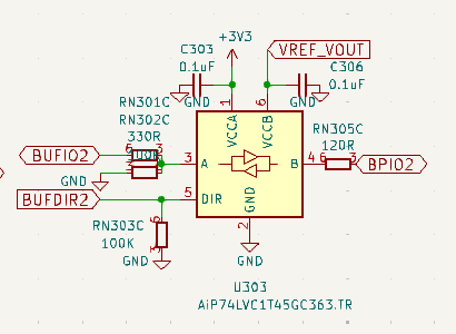
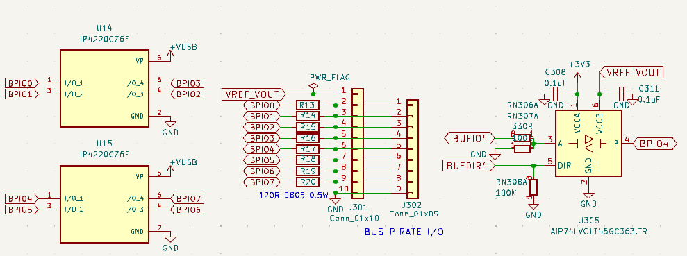
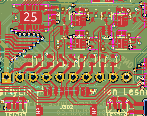
Anything that touches BPIOx moves behind a 0805 1/2W 120R thick film discrete resistor that replaces RN305C currently only on the buffer pin.

Of course, ruggedized is better and eliminates potential board problems that could complicate the user’s debugging of the DUT.

I started a REV1 board:

  • BPIOx is now an “internal” net
  • 120R series resistor (arrays) removed from 74LVC1T45 output (pin four in the U305 example), buffers output directly into the BPIOx internal net now
  • BPIOx connects to the “outside world” headers through discrete resistors.
  • Addition of IP4220CZ6F

Think this might be a preferable part due to smaller package, and as a bonus lower capacitance.

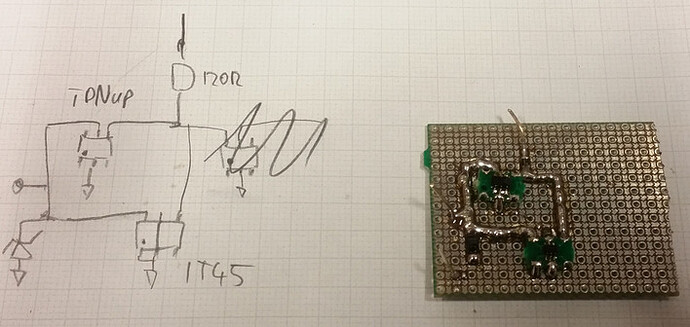
So before starting with the VOUT protection I wanted to verify the IO-port protection first and made a little mockup on protoboard:

Very good news: with the IP4220CZ6F (Nexperia) and a SMF5.0A (Littelfuse) I could protect a 74LVC1T45 (Diodes) up to 24V. The 120 Ohms resistor (0805) got up to 150°C by then and started smoking, but survived for a few minutes. Permanent 12V was no issue and no smoke. The 24V were much more than I was shooting for, so I’d call this a full success.

The bad news is that the TPNUP4202W (Tech Public) is unusable. Their datasheet is plain wrong and they don’t have the correct diodes + zener config that they show in the datasheet. It looks like a setup with individual zener diodes instead from my measurements.

So when you really want a TVS array in SC-70, you will have to look for something else. The Onsemi NUP4202W comes to mind or Littelfuse SP3002-04JTG. But I haven’t verified them. There are a few other Chinese manufacturers that have a part called “NUP4202W” on LCSC, but after this experience I’m not sure which of them have the correct configuration.

Too bad, I had planned to use a bucket of Tech Public TPNUP4202W in an upcoming project of mine. Now I have to order a bouquet of samples and see which one is true to it’s datasheet…

1 Like

Additional idea: if you have like a millimeter more space for the 0805 resistors: don’t use the default Kicad footprint, but extend the pads out like 0,3mm in each direction.

This will improve heat dissipation. But primarily it will make replacing them much easier should they ever get fried. 0805 with larger pads is something I’d say even someone without much SMD experience and a mediocre soldering iron should be able to replace.

1 Like

Oh, I forgot I also tested above IO-protection in negative direction:

I was able to turn the voltage up to about -17V until the resistor started to burn up.

Since the diodes have to conduct right from the start in this configuration (and not from about 6V as in positive direction), this is about to be expected.

So basically the “hand solder” version of the footprint.

Thank you for testing the tech republic part. Smaller would be better with limited board space, I’ll have a look.

2 Likes

image

Is there a reason not to connect the opamps to the TVS protected net?

image

I’m fine either way, but it looks like the board routing will be simplified a bit if they stay on the TVS protected net.

On first glance it looks like calculating the impedance of the DUT on a port would be easier if the ADC input is not behind the resistor. But I guess a bit of calculus shouldn’t be that much of a burden.

But I think when changing to another ADC where you don’t need Opamps in front will mean that the 100k resistor will have to shrink substantially. Something like 1k or 470 Ohms when you look into the suggested schematics for the TI part. Then there is no way not to connect the ADC input to the TVS protected net.

Also you could reconsider if you really need the BAS40 then. I think you can leave them out and still get a good protection for the Opamps/ADC-inputs this way. So even more parts & space saved.

It would be great to open up space, but will the TVS fully protect the op-amps from back powering?

My understanding is that the opamp specs +/-0.3 volts (sometimes +/-0.5) max from either supply rail. The 100K resistor limits current to what the Schottky diode can shunt to VUSB and keep the voltage under 0.3volts when the Bus Pirate is unpowered. This keeps the opamp input pin within the max limits when power is applied to the pin when the Bus Pirate is not powered.

image

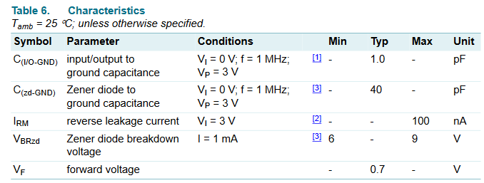
The Zener in the IP4220CZ6F breakdown is between 6 and 9volts, and the (I assume other diodes) Vf is 0.7.

I could be completely wrong, I have not worked with TVS diodes before.

  • Stick with IP4220CZ6F
  • Make 0805 Rs hand solder footprint (done)
  • Attach opamp inputs to unprotected BPIO net

For digital circuits this is most often the case. But Opamps are different in that regard as most of them have fully characterized integrated protection diodes. Look into the datasheet of the one you are using, usually you’ll find something like that you are allowed to exceed the ±0.3V spec if you limit the current to ± 10mA.

And together with the 100k, these ± 10mA allow plenty of overvoltage. And then the resistor/TVS combination will limit the input to something like 7V, at least this is what I measured yesterday.

So in my opinion you can remove the diodes from the Opamps.

Also you are working on a test revision, where you can accept design risiks in order to find out if some design improvement is possible, right? So I suggest to take this risk and try it out.

Don’t forget the SMF5.0A, it had a lower breakdown than the IP4220CZ6F in my measurement yesterday.

3 Likes