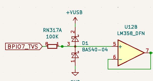
Probably best add a second SMF5.0A to VREF_VOUT until I’ve come up with a better protection scheme for it.
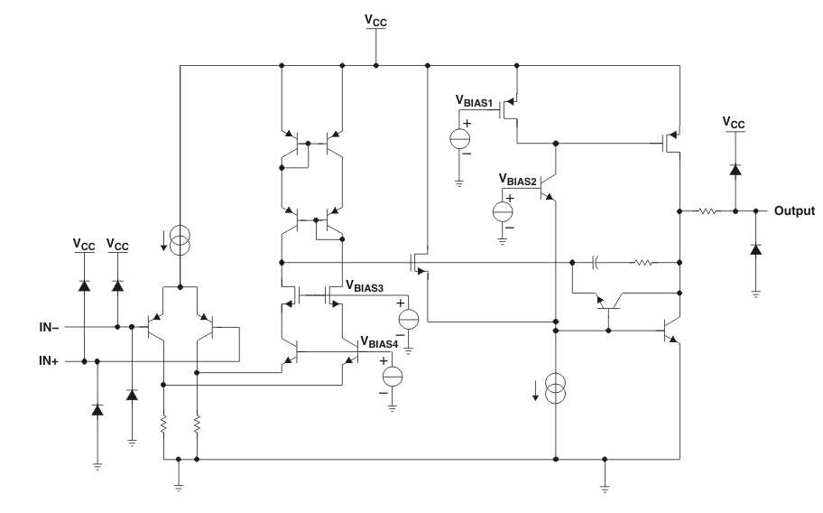
Wow, so I’m wrong on a few things. The Chinese parts have skimpy datasheets and don’t mention internal diodes. I will gainsil directly. Here’s the TI LMV324 and the diodes are obvious.
I learned about opamps from old dusty books and ancient app-notes. One of my “beliefs” is that the pins had diodes to ground, but an external diode was needed to Vcc.
To check my sanity, I pulled the datasheet for TI LM324 (no V) which is an older part. Look at that, only diodes to ground. I’m glad I didn’t make that up out of thin air ![]()
Assuming the gainsil parts have pin diodes (I will measure the voltage after the R with the D removed soon, assume it should be one diode drop?), then all of these BAS40-04s are redundant. That will save space and reduce complexity right where we need it.
Thank you so much for expanding my knowledge of opamps.
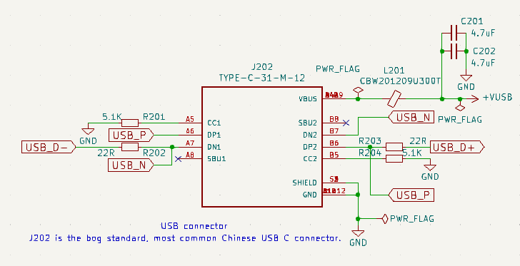
It occurs to me that we’re using USB TVS diodes, but our USB isn’t being protected. Perhaps TVS diodes after the 22R resistors on USB_D+/-?
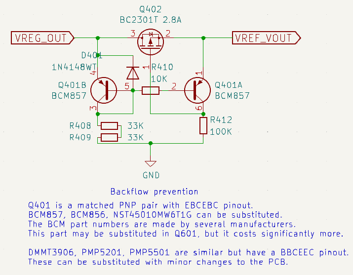
Armed with this new knowledge, there is a variant of the backflow switch that uses an opamp instead of the closely matched PNP pair. This part is expensive (relative to our BOM) and as you noted I believe it is a 5volt max part.
From this post I saw on Hack a Day years go and informed the current design. I decided against going the opamp route, for reasons I no longer remember, but probably I wasn’t confident I could protect it during partial power down situations.
As you discussed, the main limitations of the current mirror design are its quiescent current consumption and battery (reverse) voltage limit due to Q1 Vbe_max (usually -5 or -6v which limits the battery to roughly 5v6 or 6v6).
The op-amp solution to extend the voltage range is particularly nice for its very low power consumption. The LT6003 is pricey, but there are lower-cost op-amps that should do the trick too: TLV2401IDBVR (880 nA) or TLV9301IDCKR (150 uA). However, any op-amp is going to cost significantly more than the current mirror.
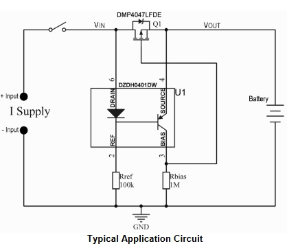
A solution that supports higher voltages and costs nearly the same as the current mirror is Diodes Inc. DZDH0401DW-7 (~$0.10 in qty 1K); current consumption is better than the current mirror (147uA) and it easily supports Vbat up to the FET’s Vgs_max (typically 12-20V).
A 2024 comment on that post leads to the DZDH0401DW, which seems like half way to protecting VOUT in general, but with a trick or two:
- Max Input Voltage: 40V
- Peak Bias Current: -300mA
- Max Reverse Voltage Protection: 50V
1 Like
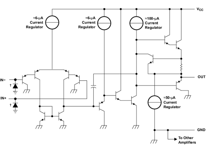
Found the origin of the diodes. The is the datasheet for MCP6001, which is the opamp we used in the first 5 or 6 revisions.
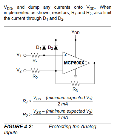
It is a modern low voltage, low power, rail to rail, but seems similar to the old LM style opamps.
1 Like
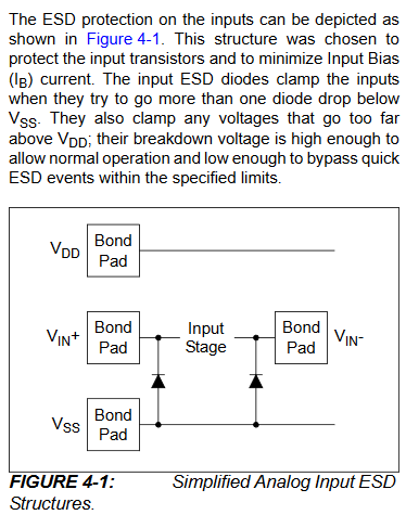
Ah, yes, this is using a not-so-well protected kind of input configuration. They claim they do it to reduce the input bias current.
They really reach low values for Input Bias Current this way with ± 1 pA at 25°C. While they advertise it as a general purpose opamp, it is well suited for very high impedance stuff like thermocouples or PH-sensors or similar this way. So I’d say it is more specialized in this direction without telling you so.
The LMV324 is more what I’d call “general purpose”. It has the better integrated protection circuitry, but the Input Bias Current is typical 11 nA (TI datasheet). This is 4 orders of magnitude more.
So as with all this stuff the exact datasheet of the part you use matters and there are differences. And then there are datasheets that are plain wrong, like the TPNUP stuff I hit yesterday.
1 Like
It had super good availability during the supply chain crisis in a small package as it’s a bit expensive and not drop in compatible with common opamps. It is also super low power I believe, and generally overkill for what were doing. I swapped to LMV3xx when doing final sourcing for the production version.
It makes sense then that they leave them out so you decide how much leakage current and input bias you can tolerate in your design. Interesting.
1 Like
Do you have a spare opamp of your Gainsil ones at hand? Maybe some left over on a reel in your office in China?
In desoldered state I’d say the best way is to use the diode test function of a multimeter and measure an IN+ (or IN-) to Vcc and GND. There should be one diode drop in each direction.
You can’t do this test reliably while the opamp is soldered onto a PCB with other components.
But it just tells you if there are diodes at all. It doesn’t tell you if these diodes are designed in a way that they can reliably conduct 10mA (or some other value) without getting damaged. So better ask the manufacturer about this.
yes, adding one of the TVS arrays to the USB port makes very much sense.
I’d say it makes more sense to put it in front of the 22 Ohm resistors in this case. Because in contrast to the port inputs, you expect more ESD events and less long-term overvoltage here. Also the 74LVC1T45 are more robust than the USB pins of the microcontroller, so having extra resistance in there helps.
If you worry about the space for the extra TVS array: I ordered several TVS array samples in SOT363 from different manufacturers. I hope they wlll arrive next week or so and then I’ll try them out.
Why are you using 22R resistors on USB D+ / D-? IIRC the Raspi datasheets recommend to use 27 Ohms.
22R I assume came from the PICO board, but I checked and pico and pico2 both use 27. Will update that.
I didn’t think I had any of the opamps, but I actually do have some SO14 chips we’re going to decap at some point.
It appears there are diodes from ground to Vin+/-, but not VCC. 0.78 volt drop or so. I imagine here this is also how they get such low offsets compared to others.
It will be interesting to see what Gainsil says. There is a GS324 and GS324A that is identical on spec (and data sheet as I recall) but slightly more expensive. I wonder if it has the diodes.
1 Like
Are these the same Gainsil GS324 you are using on the BP, just in a different case or is it a different model?
I don’t think the diodes affect the offset voltages much. Because the diodes are not conducting in normal use. The offset voltages are measured with a low-impedance source, so a bit of leakage doesn’t matter for this figure. The offset voltages are mostly caused by the internal transistors having slightly different gain and being not perfectly matched if I’m not mistaken.
But what the diodes affect is the Input Bias Current. The Gainsil GS324 claims ±1 pA for this, just like the Microchip one you posted earlier. This very much looks to me like they don’t have integrated series diodes. So you were correct in keeping the protection diodes.
1 Like
I’m moving this question from the Rev7 features thread to here because I think it is best covered here.
Now the series resistors are 120 Ohms. Is this the optimal value or would for example 68 Ohms be better?
Regarding the wanted usage I mentioned at the beginning of this thread I see mostly these points affected:
- driving old-school TTL: a fanout of 10 is common, this means you must be able to drive 16mA and keep the high-output between 5V and 2V while doing so. When we account for marginal Vusb and drop in the voltage regulator, the drop in the resistor should be below 2V. 120 Ohms gives a drop of 1.92V - so we are fine with 120 Ohms or below
- driving I2C in Fast mode plus: This means we must be able to sink 20 mA and keep the voltage at the input below 0.4V while doing so. This means our whole resistance must be below 20 Ohms. Since the 1T45 already has an impedance in the range between 10 and 20 Ohms achieving this means we can’t use more than something like 5 Ohms as series resistor. This would severely affect any protection goals. So I think we have to scratch this goal and restrict us to I2C Fast Mode (400 kHz max.).
- fast digital IO: The 25 MHz I mentioned above shouldn’t be affected by 120 Ohms. Since Rev 7 will have a PSRAM one could want to fully utilize it for a fast logic analyzer or similar. But I’m not sure what kinds of speeds are realistic there and if they are really affected by 120 Ohms.
- fast PWM or clock output: a PWM that utilizes the max. freq of the RP2350 for very short LSB times. Or a clock output with high frequency. This could be intersting for some use cases and the 120 Ohms will affect you for example if you try to go to 75 MHz (half MCU freq.)
- The point of protecting the DUT is a bit difficult because it is a goal of the BP to interface with as many different kinds of DUTs as possible. So very different requirements and kinds of damage level.
So I don’t see a clearly defined & realistic feature that is not possible with 120 Ohms. But the lower the resistance, the more speed is possible, but the protection becomes more difficult.
To test the resistor effects on the protection, I used the protoboard circuit from yesterday and replaced the 120 Ohms with 100, 82 and 68 Ohms:
Interestingly the voltage the resistor started smoking at didn’t vary much. It was always about 24V. But the lower the resistance, the more power the TVS diode array and SMF5.0A had to carry. With 120, 100 and 82 this was still fine at 24V, so the resistor was the limiting factor. With 68 Ohms this changed and the TVS diode blew at 20V.
In the end I think there is no optimal resistor value we could calculate, it is guesswork and eyeballing. I think 120 Ohms should be fine, but it could also be slightly lowered to the more common value of 100 Ohms. But I wouldn’t go far lower unless some real issue with the series resistor comes up.
1 Like
Gainsil claims the opamps have diodes in both directions. I’m almost completely sure they don’t. I took photos of the multimeter test and will talk to them tomorrow.
At least they answer you at all. At many western semiconductor companies you need an assigned FAE (and the sales volume to back that) or all your emails directly go to /dev/null.
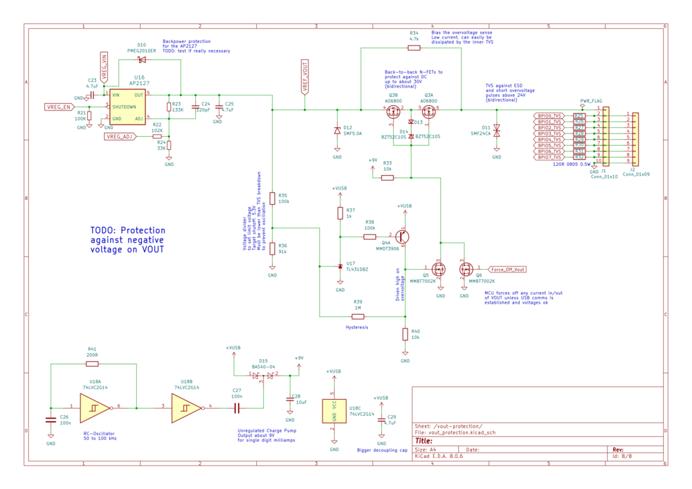
So I’ve been working on a protection for overvoltages coming in via VOUT and I want to show my current progress:
vout_protection.zip (24.1 KB)
Current state is that I haven’t implemented a protection against negative voltages (aka reverse polarity protection) yet and it is not tested or simulated yet.
I chose to use N-FETs and create a 9V bias voltage with a small charge pump for them:
- N-FETs are better than P-FETs, so easier&cheaper to find
- The charge pump is small & cheap (74LVC2G14 is available in SOT-363)
- We want it to work down to like 1.2V, a P-FET would have to use that as gate potential and wouldn’t be fully conducting then. There might be some that work down in that region, but they will then have very
sensitive gates that become hard to protect during fast voltage transients. - A N-FET switched with 9V will have a ~4V gate potential at 5V, so will conduct fully
- When the charge pump is off, the back-to-back N-FETs will fully block all current, so we get a proper protection for the unpowered state
When this is finished it will also replace the current backflow protection. This his how/why:
- Current backflow protection protects the USB Host / PC when you have a power supply connected to VOUT but the USB Host / PC is switched off or you inject a voltage above 5V via VOUT.
- The new VOUT protection will prevent voltages dangerously over 5V reaching the voltage regulator, so also the USB Host / PC.
- So we just need some protection for the case where the BP was powered, it activated the charge pump and opened the VOUT protection, but you then switch off the USB Host / PC and the BP keeps running from the external power
- This is where the Force_Off_Vout signal comes into play: When the USB link goes down (or is not up yet), the firmware can activate it and switch off everything coming in via VOUT. This will prevent any current from reaching the PC
- This means we don’t need an extra backflow protection circuit anymore
- The only thing that needs to be checked if we need a diode across the AP2127 voltage regulator or not. The datasheet doesn’t say. But it could very well be that there are body diodes inside that implement that function.
So getting an extra pin on the RP2350 for Force_Off_Vout would be optimal. It would also give more control over VOUT and when the io buffers are powered or not. But if there is no free pin at all it could also be emulated by a small RC trigger circuit that looks if for example the I2C clock or SPI display clock is toggled for some time. If not, then VOUT is switched off. This would then just be for the USB unconnected state and not allow dedicated software control.
@ian do you like the direction this is going?
Sorry the image above is so difficult to read. I tried to upload the image in better quality, but the forum software automatically downscaled it. And pdf files are forbidden to upload.
So here is a zipped pdf:
schematics.pdf.zip (81.9 KB)
But the original kicad file in zipped form is also in the post above for those that have kicad installed.
1 Like
Here is an updated version that includes protection for negative voltages.
vout-protection.zip (134.3 KB)
I changed the TL431 that I used as comparator + reference in yesterdays version to a LM393 comparator. The TL431 solution was something that I have used before for similar circuits, but just in positive direction. This is why I first started the circuit with it. But the LM393 allows to easily do the negative voltage detection. Also the LM393 is available in QFN 2x2 so it is smaller.
@ian what do you think about this circuit? Has this a chance to go into Rev7?
Then I offer to build up a sample on protoboard to verify it actually works as planned.
1 Like
Wow, this is super impressive. I’ll tentatively add it to the schematic. We finalized the new case tooling today so I haven’t been as active as usual.
I’m sorry about the forum limitations, it is on my list of things to look into. I need to move everything over to an S3 bucket or something.
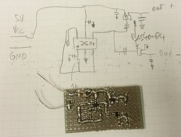
So I started building up a sample. The charge pump for the aux voltages was first:
No surpises, the circuit works as expected for such an unregulated charge pump:
Positive output at 5.0V in:
0 mA load: 9.5 V
0.5 mA load: 9.3 V
1 mA load: 9.2 V
2 mA load: 9.0 V
3 mA load: 8.8 V
Positive output at 4.5 V in:
0 mA load: 8.6V
0.5 mA load: 8.3 V
1 mA load: 8.2 V
2 mA load: 8.0 V
3 mA load: 7.8 V
Negative output at 5.0V in:
0 mA load: -4.6 V
0.5 mA load: -4.3 V
1 mA load: -4.2 V
2 mA load: -4.0 V
3 mA load: -3.8 V
Negative output at 4.5V in:
0 mA load: -4.1 V
0.5 mA load: -3.8 V
1 mA load: -3.7 V
2 mA load: -3.5 V
3 mA load: -3.3 V
The positive output will be loaded with only like 0.1 mA when the protection is not triggered and the FETs should conduct - we get the maximum voltage out of the charge pump then and this perfectly fits: Vgs will be between 4.5 and 4.1 V on the FETs, so they will fully conduct. When the protection triggered, we will draw like 0.9 mA.
The negative output will be loaded like 0.6 to 0.8 mA with the idle current of the comparator in the non-triggered state. In triggered state the 0.9 mA will be added, so about 1.8 mA. Since we just must go a bit below our diode drop and keep up the diode-biassing, I don’t worry with these numbers.
I used caps in 0402 where it matters, so the dc bias effects should be similar to what we’ll see in the final circuit.
You might see the ground spring I soldered in the photo. I used that to measure the ripple on the input supply with a scope. I was in the order of 20 mVpp. But it wasn’t very conclusive. The circuit loops are gigantic compared to what would be on a PCB, so my guess is that most of this ripple just comes from the abysmal layout.
Only downside is that such a regulator is quite inefficient. Just the oscillator and buffer at 5V, without any of the diodes connected, draws about 20 mA. But it will probably go down with a better layout. When you add 2.5 mA load on each side, the current goes up to 30 mA. This could be improved by replacing the 74LVC2G14 with a pin from the RP2350 that uses a PWM-unit to create the frequency and then a 1T45 to shift it up to 5V. But unless there is an unused pin on the RP2350 left I’d accept these 20 mA extra for the protection circuit.
I will build the main part of the protection cirucuit next, but it will probably take a few days till I have time.
2 Likes
The two new pages are now added to the project in git.
I did a small cleanup of the top layer schematic. Is a top page actually still needed in the latest version of KiCAD? I’ll have a look some time.
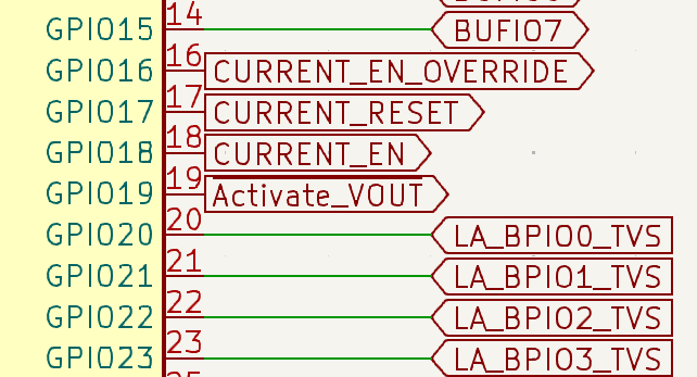
We can move the over current detect back to the analog mux, and use that PICO pin to drive Force_VOUT_VOFF (~{Activate_VOUT}).
TODO:
- Connect opamp IO buffers to BPIOx_ nets instead of TVS protected nets
1 Like
Nice, thank you.
Just don’t invest too much time with layout on the Vout-protection part yet, as I think it is not too unlikely that there might be some changes needed. For example the part around the AP2127 voltage regulator or maybe additional hysteresis for the comparator.
You’ve probably seen that I added the pullup to Force_VOUT_VOFF and renamed it accordingly. The idea being that Vout is disconnected by default, for example while you are in the bootloader.
Having this on a dedicated pin is the best solution I think, because it gives you full software control over Vout.
Today I received the parcel with 6 bags of samples with TVS diode arrays in SOT-363. I hope that at least one of them offers comparable performance to the IP4220CZ6F in a smaller footprint. I will try them out and compare them in the next few days.
3 Likes
Today I finished comparing the TVS diode arrays in SOT-363.
Unfortunately there is only one that works and it is a western part: Littelfuse SP3002-04JTG, costs about $ 0.16 @ 500pcs.
Two of the Chinese ones didn’t have the diode configuration that was shown in the datasheet (DOWO and Leiditech). The same as the Tech Public TPNUP I mentioned before.
One of the Chinese ones wasn’t robust at all, I blew several just by going to 50 mA. Another one of the Chinese ones worked, but had high leakage current (MKSEMI), so it would affect ADC operation.
I was completely surprised that the expensive onsemi NUP4202W1T2G also had such a high leakage current. I measured about 120 nA into ground at 5V. The Littelfuse instead was below 1 nA at the same conditions (the 1nA is the lower limit of my measurement, I would have to invest much more time to get a stable measurement in a lower range).
So the good news is that there is something in SOT-363. The bad news is that you have to pay about 4 times as much for it as for the IP4220CZ6F.
2 Likes