Port protection for Rev7

Great to have a know working part, and in a small package. Thank you for testing that.

Truly bizarre how bad these domestic power protection parts are. I get “tolerance isn’t as strict”, but completely missing the structures that are key to doing the thing it does, just wow.

image

Are you happy with the two TVS diodes here?

  • PESD12VL1BA
  • SMF24CA

It could be that in a big part of the Chinese market circuit protection, and properly designing and testing it, doesn’t have the same importance than for western manufacturers. Some completely leave circuit protection out, others just put anything that looks like it in there but don’t verify it fully works as expected. So the manufacturers get by with delivering only “something”, but cheap.

After this experience I’m going to try them out before commiting to one part. I also have an even smaller one on my list for the gates, Nexperia PESD12VV1BL. But getting the rest of the circuit to work is my first priority.

Regarding the FET: the AO6802 is a dual FET in SOT-23-6 that looks like it would fit and seems to be well available. Do you prefer that or should I look into small single FETs instead, like for example the PMXB56ENZ (DFN 1x1mm)?

Board space is at a premium, we should steer clear of SOT-23-x whenever possible.

1 Like

I consider building up the port protection on protoboard too much work, especially since I also want to test out the final devices, like the PMXB56ENZ in DFN 1x1mm and the small PESD12VV1BL diode.

So I’m working on a small pcb to be fabbed instead:

I included several options and possible variants. So I can try out different things, like with/without extra hysteresis or where to tap off the comparator input.

Also the IO port protection is on there again, so I can test it again, this time with the Wuxi 1T45, the small TVS diode and the final resistor.

Looks finished, but I’m tired now, so tomorrow I’ll review and send it off to production.

4 Likes

That looks good, and overall doesn’t seem like a huge amount of board space.

I’ll have a look again to see if I can eek out a pwm for the negative voltage, but I think it’s going to be hard.

I ordered my test pcb and added the charge pump circuit on the bottom. So I can test it again with a better layout. Regarding the current consumption, one reason could be that I used the “default” 100nF for the RC circuit, meaing the 100nF have to be charged and discharged each cycle. I will try with much lower values like 100pF and increase the resistance instead. Also I can try different frequencies, this could also have an effect.

So maybe the self-oscillating circuit can be improved enough that you can sleep peacefully without needing a PWM from the RP2350.

1 Like

We were able to source RP2350B chips in the market today. After Spring Festival we’ll have the first revision of BP7 prototypes made in a small batch (5? 10?).

1 Like

Sorry for taking so long to finish this. After the usual pre-christmas-craze at work I had to deal with some family business and then the provisional mains wiring on my workbench I put in like 5 years ago finally broke down. I finished properly re-wiring my workbench yesterday and now it is a dream work there - I should have done this much sooner…

So I started populating the test pcb. The first part was the aux voltage regulator for 9V and -5V:

With a proper pcb with short traces and good ground the idle load went down a lot, as was to be expected. With 100nF and 200R I got 7.8mA. But as I guessed this could be optimized a lot by going to 100pF and 200kOhms:

With this the idle consumption went down to 2mA. I think this is totally acceptable, so we don’t need a precious pin from the RP2350 for this.

The 74LVC2G14 oscillates with about 50 kHz. With just a 10µF cap on each rail the ripple on the output is negligible and doesn’t need any extra filtering with the expected loads.

The main Vout protection circuit comes next.

2 Likes

First light :bulb:

This is the io voltage (VREF_VOUT) at 5V from the outside (VOUT):

And this is what happens at 30V from the outside:

No fire or smoke, just the mosfets switching off as they should.

This is with the most basic way of wiring up the circuit. I left out all the extra provisions for stronger hysteresis and so on.

There are many more tests to do in the next few days, but this looks promising.

3 Likes

Next point to check: How does the AP2127 voltage regulator behave when backpowered, as in Vout > Vtarget and Vout > Vin?

This is of concern when you have set the regulator to output for example 3.3V, but you apply a higher voltage to VOUT, but one that isn’t so high that the new protection circuitry is triggered yet.

Also the Vbus you power the Bus Pirate with could be exceptionally low, for example 4.5V, and you then apply say 5V to VOUT. So Vout > Vin on the regulator.

Unfortunately the datasheet doesn’t say one word about this.

So I tested it:

  • When Vout > Vtarget no current is flowing backwards through the regulator
  • When Vout > Vin+0.5V a current starts to flow from Vout to ground. This looks very much like a regular protection diode.
  • Enabling or disabling the regulator with the shutdown-pin doesn’t make a difference

So there are two ways to deal with this:
The perfect one would be an additional Schottky diode across the regulator to discharge this voltage. But since we want to save board space I try to make it work without.

Using one of the channels of the SP3002-04JTG that are already planned unfortunately doesn’t work well in this case since their diodes aren’t Schottky and don’t conduct just yet at these voltages. I think still doing this wouldn’t hurt when we have a free channel.

I lowered the threshold voltage of the comparator. I have now set 5.65V and measured about 20 mA flowing through the diode of the regulator in this situation. Since this is a power component designed to source 300mA, I hope that these 20 mA won’t overload it.

I let it run for 30 minutes with these 20 mA. It worked fine afterwards and I didn’t measure any increased idle consumption afterwards. So I’d say this is fine for this application. Probably not over the full industrial temperature range and you shouldn’t do this on some expensive satellite, but for a Bus Pirate we shouldn’t overdo it.

3 Likes

Wow good testing! Thank you.

This is all for fun, no rush! You issued a warning we wouldn’t see much of you for a month or so :slight_smile:

Would it be big hit to add a Schottky? We have BAS40 on the BOM in SOT-523, they’re pretty tiny.

You are right, SOT-523 doesn’t take much space.

I will test a BAS40 across the AP2127.

1 Like

I tried a BAS40 across the AP2127. It works by taking up the reverse current that would otherwise flow through the protection diodes of the AP2127.

But the BAS40 is usually limited to 120 mA + thermal limit. If someone were to use the BP for a longer time with an externally provided Vout at, say 5.5V and a low Vbus with for example 4.7V, then the whole Bus Pirate and other usb devices connected to the same rail would be powered through this diode. Then the 120 mA could not be enough and the diode burn out.

So to properly solve this I see two solutions:

  1. We use a stronger and larger diode, for example PMEG2020EJ that is rated for 2A. SOD-323F, so it is not huge.

  2. The ADC of the BP is used to constantly compare Vusb and Vout. If Vout > Vusb+0.3V we switch off the protection mosfets from firmware. It doesn’t matter if this takes a few µs: the BAS40 will survive for a short time, just not longer operation. Downside is that this kind of software protection doesn’t work for example in the bootloader or alternative firmwares.

1 Like

While doing further tests I found out that I made a mistake with my schematics regarding negative voltages: I didn’t realize that a n-mosfet with it’s gate pulled to GND is wide open when you have something like -5V applied to it’s source. Oops.

Fortunately I found an easy fix for this:

  1. using different resistors between gate and the two channels of the comparator. So the comparator channel that senses too high voltages keeps it’s 5.1k resistor I initially planned. This is to make it not so hard on the little TVS diode protecting the gates when we got > 20V on VOUT. The resistor for the comparator channel that senses negative voltages now gets just a 100 ohms resistor. So it can pull down the gates to very near V- of the comparator.

This solves the problem with a VOUT until like -5 V.

  1. V- of the comparator is normally the -5V supply created by the negative charge pump. But this isn’t enough once VOUT goes more negative than that. Because then our gates are more positive than VOUT and the mosfets begin to open. So I added a BAS40 diode from -5 to VOUT. So that VOUT can pull the (nominal) -5V rail to more negative voltages, but not the other way round. The LM393B works up to 36V, so pulling it’s V- to -30V while V+ sits at Vusb is allowed.

With this small modification the circuit was able to survive the full range of +30V to -30V on VOUT.

In the end I plan to additionally put a bidirectional 24V TVS on VOUT, so that the TVS begins to conduct before we hit the ±30V. This means ±24V will be permanently allowed on VOUT, with the circuit still being protected if you have short transients going above that.

The protection keeps working when the circuit is unpowered. In the positive direction you would need the 9V supply to open the mosfets, so no issue. In the negative direction the comparator has to pull the gates low to protect. But with my diode modification from above the comparator can use a negative VOUT as it’s supply. The comparator turns on enough before the mosfet begins to conduct - very convenient.

2 Likes

Now I changed the gigantonourmous SOT-23 mosfets I used for initial bringup to something more appropriately sized for the BusPirate: PMXB56ENZ in 1.1mm x 1mm DFN:

Was more easy to solder than I expected, a little hot air and they worked on the first try.

They also had no issues to survive the hole -30V to +30V range, didn’t get hot and so on. So I’d say these are a good choice.

3 Likes

I populated the IO-circuit with a Wuxi AiP74LVC1T45, a 120 Ohms thick-film resistor in 0805 and did some more testing:

  • Like in my earlier testing I could apply about 20V without the resistor smoking or other issues.
  • At 24V the resistor started smoking. But even after 5 minutes of smoking and looking a bit crusty it still survived and still had 120 Ohms after cooling off. So while not perfect, it survived long enough that you can react when you smell it. The BP would have survived fine.

The only issue is, as I suspected, when you switch the 1T45 to output mode and then overpower it from it’s output with some voltage higher than VREF_VOUT. In this case the internal transistor of the 1T45 is on, so current can flow freely in both directions.

While the resistor limited the current, the SP3002-04JTG TVS wasn’t strong enough to keep the voltage on VREF_VOUT in check. When it reached about 12V the voltage regulator broke through and was destroyed. On a real BP other parts are in danger too and could break down much sooner.

I could solve it by adding one SMF5V0A to the VREF_VOUT rail. That could keep the voltage to about 6V, which all components could survive.

I think I’ll do some transient tests next to finish off the testing, maybe scroll through the thread and check off all requirements from the beginning. But I’d say the design of the port protection looks quite good so far.

4 Likes

I’m loving seeing your progress and testing. I’ve no formal EE training, so much of the “why” behind your choices is beyond my ken, and yet I am loving the updates. Amazing!

1 Like

This is an excellent read and inspired testing, I agree.

Glad you like the updates on the stuff I do here for the port protection. Will continue to explain what I do.

I also don’t have a formal EE degree. Everything I do is self-taught.

3 Likes

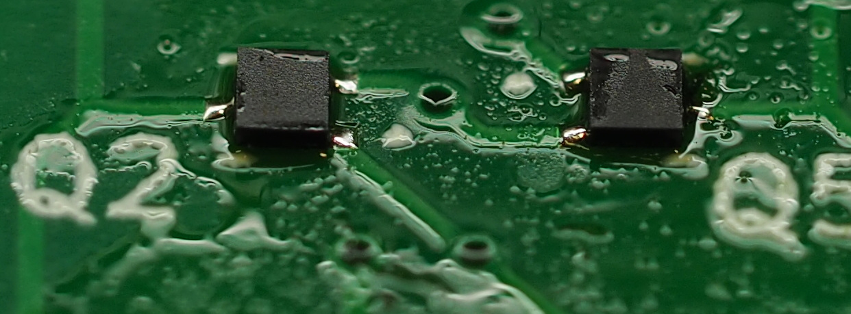
So before starting transient testing I thought I do some more testing on the two
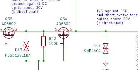
PMXB56EN N-mosfets. These will be added between VREF_VOUT (this is the internal net where the 1T45 are powered from) and VOUT (external pin on the header).

Here especially the resistance of these two mosfets could be an issue and should be checked.

We drive their gates from our auxiliary 9V (nominal) supply that is created with the charge pump. It could be that the 9V are not enough to properly open them: What matters is that the gate voltage is far enough above the source voltage, that is the voltage applied to VREF_VOUT. So if someone wanted to use 3.3V then we were 5.7V above source, which would be good enough. But if the nominal 9V aren’t 9 and someone wanted to use 5.5V then we could run into issues.

So better measure it:

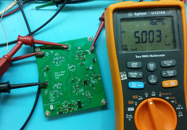
5V Vusb gives 8.7V at the gate, 4.75V Vusb 8.3V at the gate, 4.5V Vusb just 7.9V. So properly powering the BP matters.

A normal use would be for example to input 250 mA @ 5V into VREF_VOUT and properly supply the BP with 5V Vusb. The gates then are 3.7V above source - this is less than what the specification of the fets define, so the resistance will be higher. They specify max 65 mOhms per fet at 4.5 gate/source. I measured 48.7 mV or 194 mOhms for both of them.

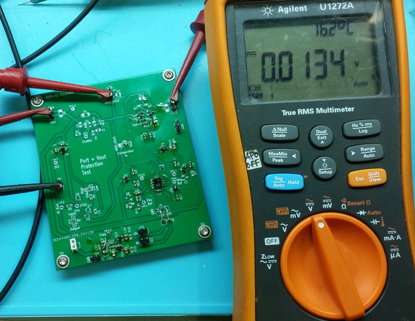
If you go up and want to input 400 mA @ 5.5V into VREF_VOUT I measured 208 mOhms. So not much of a difference in this direction.

When the host you power your BP from is supplying you less voltage then it goes up though: with 4.75V Vusb and 5.5V input I measured 237 mOhms. If your host just supplies 4.5V Vusb and you then want to use it goes up to 345 mOhms.

But all these vales still just mean you lose about 100 mV. When you supply the VOUT from the outside for example from a lab psu you probably can easily compensate that by just going a few mV up if it really matters.

When the power goes the other way and is supplied from the internal voltage regulator you obviously can’t go above Vusb and also have to live with the like 100 mV drop of the regulator. So your source voltage isn’t as high to start with and this helps getting the gate-difference higher.

If you set the voltage on VOUT to 3.3V there should be enough difference to the gate, more than 5V. But I still measured still 179 mOhms over the two fets. This is 89 mOhms per fet, so quite a bit more than the 65 mOhms per fet they claim in the datasheet. Now there are of course contact resistances on my pcb and measurement setup, but I wouldn’t expect these resistances to be so high. But I’m not in the mood to hunt these milliohms down, since I think they don’t matter much in this usecase.

I think these fets will work well for this case and the extra resistance is a price you have to pay for the extra protection.

2 Likes