Port protection for Rev7

Good update. I’m glad you tested down to 4.5. We had a test computer in the office that frequently failed self tests because VUSB is 4.6-4.7.

Over the years I’ve seen a lot of bus pirate selft test fail because VUSB was too low. Never because it’s too high though :slight_smile: This seems less and less common though, laptops especially have much more consistent 5V rails.

On to transient testing:

Positive spikes first. I used my bench power supply, set it to the wanted voltage, enabled it and then touched the positive output wire to the VOUT-pin. So there is the (smallish) output cap of the PSU charged to the set voltage and the contact bounce at play.

Lets see how my protection circuit mockup reacts to that.

I will start with the lower end of where the protection circuit reacts first. This is interesting because:

  • the comparator reacts more slowly near to the threshold
  • hysteresis issues would show up in this region if they are there
  • the SMF5.0 TVS-diode that we added to VOUT_VREF could somehow interfere with the comparator threshold and cause oscillations

5.70V:

5.80V:

5.90V:

6.00V:

6.00V zoomed in to the first trigger:

As you can see there is some bouncing back and forth going on at the lower voltages. This gets less and less the higher you go - the comparator reacts faster then.

Does this look pretty? No.

Is it an issue? No.

The important part is that the protection is active at the end (gate low) and there is no constant oscillation going on. It always becomes stable after like 100ms.

2 Likes

Next transient test:

Does VOUT_VREF (the “inner” voltage) ever reach dangrously high levels, even when you connect a charged capacitor? Or does the protection react fast enough to prevent that?

I connected a 470µF low-ESR polymer cap to my bench-PSU, configured 30V and touched the positive leg of the cap to the VOUT pin:

Here is a zoomed in screenshot:

I saw some small sparks fly, but as you can see in the cursor measurement VOUT_VREF didn’t rise above 5.8V.

So I’d say this is a full success.

Negative voltages next.

3 Likes

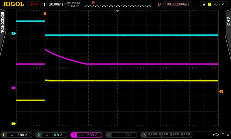
For the negative voltages I first played with -0.5V to -1V and -5V. No real differences there - some contact chatter and the protection reacting.

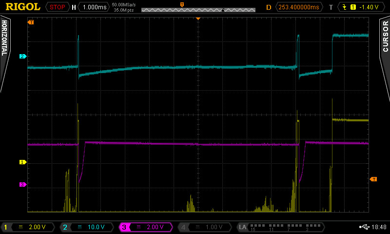
Here for example -5V:

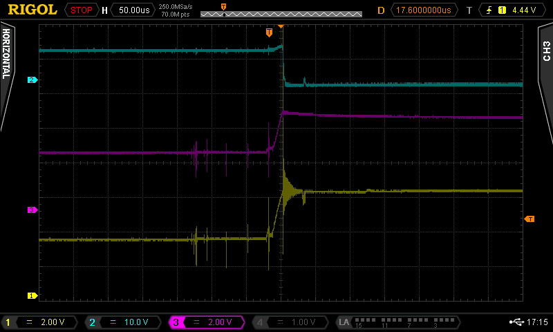
And zoomed in to the contact chatter:

As you can see the VREF_VOUT never ever even goes slightly negative - perfect.

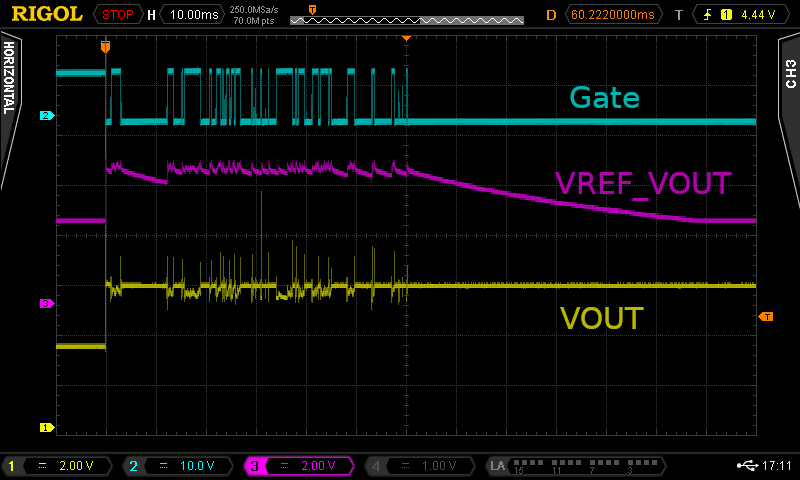
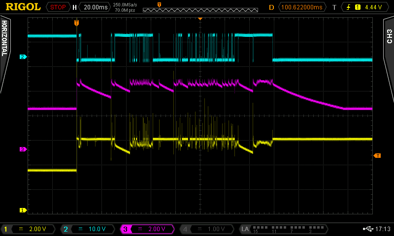
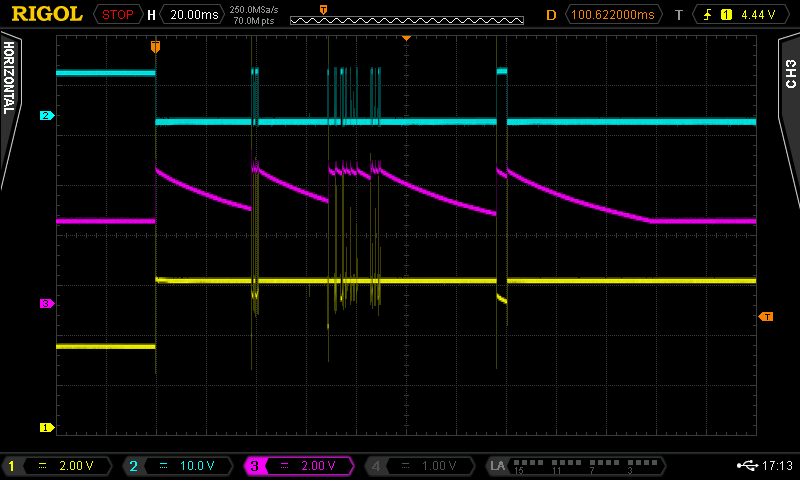
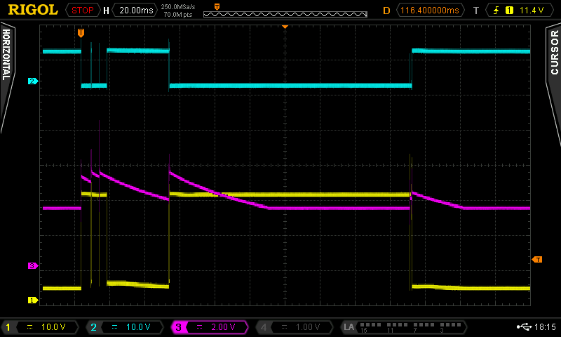
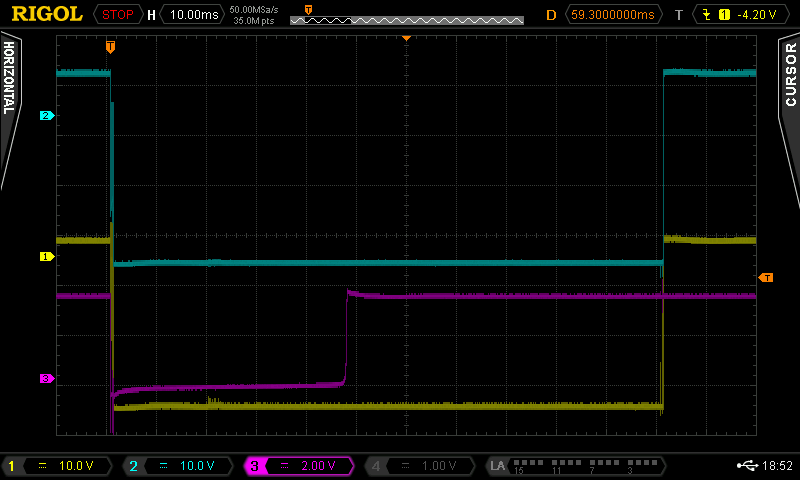
Now I got out the “big guns” and connected my 470µF low-esr polymer cap again. Connected to the lab PSU at 30V and wired up for negative voltages, then touching the leg of the cap to VOUT looks like this:

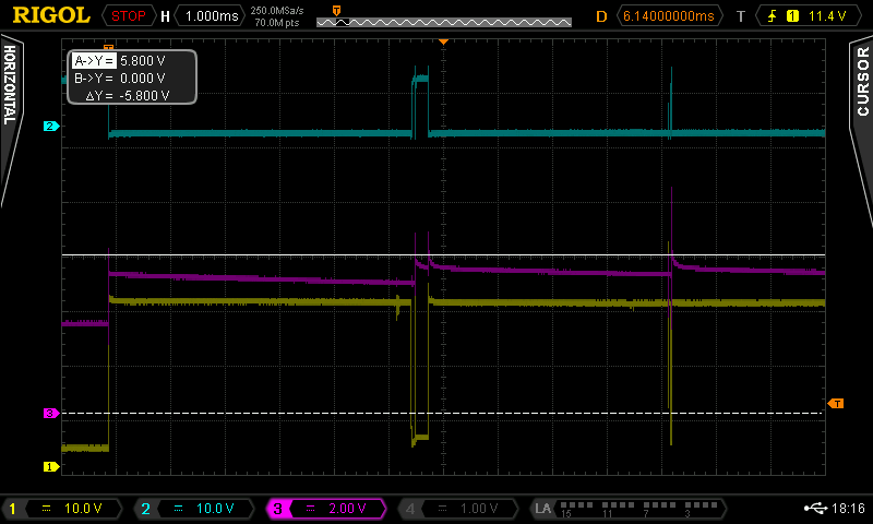
Zoomed in to the first contact:

I saw a bigger spark fly when touching the cap.

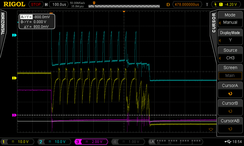
Now this is more interesting to analyze!

Let’s start with the non-zoomed version first. On the big scale the circuit reacts as designed. VOUT_VREF is hooked up to the voltage regulator, configured to 3.3V. It looks like it’s regulation circuit gets “shocked” a bit and it takes some time to recover and enable the 3.3V out again.

On the zoomed in version the most important thing is how low VOUT_VREF goes. -800mV is not perfect, but this was the most stressful test for the whole circuit. A bit less would be better, but I guess the components will survive. I think the SMF5.0A TVS-diode is the one that limits this voltage first before the gate voltage drops and the mosfets close.

Then we have this oscillation phase going on for about 600µs. My guess is that the capacitor gets discharged quickly, due to the TVS activating. You can see in the yellow trace (VOUT) that the voltage rises from nearly -30V to about 0V. The protection then disengages, the gate voltage rises. Then VOUT falls again and the cycle repeats. I guess this is the regulation circuit of my lab PSU reacting. Also the negative supply voltage and it’s capacitors of the comparator has to be discharged.

All this could be amplified by contact chatter: as I touch the leg of the cap to the VOUT pin there is no stable electric contact. So we have some contact resistance. As I see quite a spark, small particles vaporize and we get a higher contact resistance. This allows the PSU to charge the cap again without hitting the current limit.

Once the physical contact is stable after like 600µs the situation stabilizes.

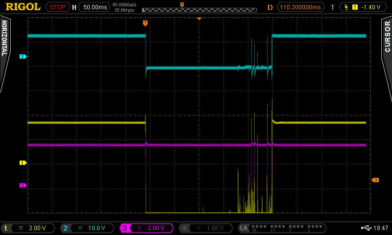
I repeated this like 50 times in short and longer succession, with different current settings on the lab psu and so on. Apart from the sparks I did not see any adverse effects, the circuit survived.

So I’d consider this test passed too.

3 Likes

Great stuff to learn thanks for that @electronic_eel

2 Likes

Next question: do we need extra protection against ESD and similar fast transients on VOUT?

Unfortunately I don’t have a proper ESD gun that outputs the impulses used in the EMI norms - these guns are quite expensive, even used ones can go for like 10.000 EUR. So I have to improvise with a piezo grill lighter. It emits more powerful pulses, but not so fast ones.

I fired like 10 pulses onto VOUT and the mosfets and the diode to the negative opamp supply were dead.

So yes, we need additional protection there (as I already guessed).

I had planned a SMF24CA for this, but haven’t populated it yet for my tests.

I now added the SMF24CA and replaced the mosfets and diode.

I fired like 20 pulses and again got a problem - the mosfets survived, but the diode was dead again.

This is an issue with my layout: The diode was a bodge added later on. For convenience I soldered it directly to the VOUT pin, that is where I fired the pulses to. The SMF24CA is a few millimeters away from that, in the direction of the FETs.

So I replaced the diode again and soldered the connection to the diode behind the SMF24CA.

Now I was able to fire 50 shots and didn’t get any damage.

So, to conclude, the SMF24CA is necessary and the layout matters.

2 Likes

I re-read this whole thread again and didn’t find any loose ends and stuff to test. So I’d say this is ready to be incorporated into the Rev7 schematics.

@ian how do you prefer to go about this?

Is a pull request based on BusPirate5-hardware/pcb/7-REV1 at main · DangerousPrototypes/BusPirate5-hardware · GitHub ok?

Or do you have some local changes that you haven’t pushed there yet?

Or do you prefer some other way?

3 Likes

This made my day! This was some good testing. I really enjoyed how moving the TVS closer to the FET made such a difference. Placement matters!

I came here to re-read the thread and try to piece together everything to update the schematic. However, if you are willing to do it, please do. It will be a lot more accurate that trying to wrangle everything back together from the thread. I checked and there are no new changes to push.

EDIT: After the schematic is updated I will make a supplier sheet and also send the board for routing. Depending on the routing time, we may have these in hand within a month of REV0. That should give us time to test some of the new subsystems and make any last minute tweaks.

For example (off topic): I imagine we might want a 100-200ohm pull-x resistor option to eg check for power and ground pins.

Yeah, I guess when you do it it will be a lot of back and forth until we get everything right.

So pull request it is.

1 Like

With the current configuration we can already get down to IIRC 1.2 kOhm or something. We have an accurate ADC to measure the effect and don’t just have to rely on the digital high/low, so I think we are already fully capable to measure in the low-impedance area of power and gnd pins.

So I was thinking if we shouldn’t change the setup to include a more high-impedance resistor, allowing to better distinguish pullups/pulldowns in the 100k to 1 Meg region.

But this is exactly the kind of question why I like the gradual Rev7.0/7.1/… approach - we can easily test this out and improve.

1 Like

Agree with all you wrote.

This also occurred to me a while ago and I spent a day making notes and spreadsheets. Ultimately I decided the solution would probably reveal itself during dog-fooding.

1 Like

You got a pull request Port protection for Rev 7 by electroniceel · Pull Request #1 · DangerousPrototypes/BusPirate5-hardware · GitHub

I tried to separate all the changes into small separate commits. So you should be able to review them each with a graphical diff tool if you want.

1 Like

Repeating this for a list of changes before routing.

  • 7002 size change is a good update, especially not that there are more than 1 per PCB.
  • I don’t see anywhere the 2.2uF would be critical, these should go to 4.7uF (changed, but not pushed)
  • The DACs specifically spec a 10uF 0805 cap, we could replace the 0402 10uF in the charge pump with one of those and reduce the BOM?

New parts to source:

Quantity Part package Manuf.
1 74LVC2G14 SOT-363 WuXi I-Core ~0.5kuai
1 LM393BIDSGR WSON8 2x2mm TI ~0.6kuai
1 SMF5.0A SOD-123F Little Fuse ~0.5kuai*
2 PMXB56ENZ DFN1010 Nexperia ~0.84kuai
1 SMF24CA SOD-123F Little Fuse ~1.2kuai*
3 SP3002-04JTG SOT-363 Little Fuse ~1.1kuai**
1 PMEG2020EJ SOD-323F Nexperia,115 ~0.6kuai Nexperia ~0.78kuai
1 PESD12VV1BL SOD-882D Nexperia,315 ~0.2kuai

* There are off brand parts for these TVS diodes, but I believe you’ve tested them and found them unusable.
* * There are off brand parts for this USB TVS, but I know for a fact you tested the alternatives and found them lacking.

CBI 2N7002KT SOT-523-3 has equal or better specs that the CBI MMBT7002K SOT-23 that we currently use.

Yes, sorry, you are correct, we are crossing multiple topics.

REV0 is going as is (with the poorly done TVS not populated). It is already in production, it’s a done deal.

I was following onto your REV1 push with comments about the protection parts, but this should indeed be in the other topic. Discourse doesn’t have a way to split or move posts between topics that I’ve found, or I would reshuffle a bit.

Ah, ok I missed that the charge pump was already 0805.

I saw you had already made this change and assumed you meant the remaining 10uF on the charge pump. I’m sorry for the confusion.

SAMSUNG(三星) CL05A475KP5NRNC

I fear you didn’t look closely enough:

  • SMF5.0A is also SOD-123F, not SOD-123
  • 1x PMEG2020EJ, SOD-323F
  • 1x PESD12VV1BL, SOD-882D

Yes, the CBI 2N7002KT should work well.

1 Like

Thanks.

I used this tool from Samsung to compare yours and mine:
https://weblib.samsungsem.com/mlcc/mlcc-ec.do?partNumber=CL05A475KP5NRN
You need to double-click the part number in the search window and then enable the graphs in the top section before it works, their UI always confuses me.

Here are the relevant comparisons at 3.3V and 5V:


The blue lines are yours, the red ones mine.

So as you can see the red capacitance is higher at both voltages, the impedance lower. Yours can just go up to 10V (with nearly no capacitance left though), while mine is just rated for 6.3V max.

So I would suggest to replace all your 4.7µF parts with the 10µF CL05A106MQ5NUN. Cost should be about the same.

We still need a 10µF in 0805 of course for the 9V aux voltage and the DAC.

1 Like

Thank you so much! Table updated. I made the list while checking the schematic, rather than a BOM export. Just at the curiosity stage.

I assume you’re using Nexperia for those last two parts. They come in several versions, but the datasheet is identical. I believe the difference is reel size or sloppy data entry on SZLCSC’s part.

Yes, I tested with Nexperia.

There are different diodes with different characteristics available as PMEG2020, like PMEG2020EPA, PMEG2020EJ, PMEG2020CPA and so on. So these last letters matter. Same for the PESD12VV1BL.

1 Like

Do you like this proposal?

If yes, please push your changes and then I could change over the capacitors, review them that we have the sizes correct and send a pull req.

Just to not confuse anything, this would be for BP7 Rev1, before the new layout is started.

1 Like

Pushed changes:

  • All 2.2uF, 4.7uF → 10uF/6.3V CL05A106MQ5NUN
  • Reverted value of boot/reset resistor for 10uF cap
1 Like