Maybe it wasn’t a genuine LOTES socket? They usually have a good reputation, I wouldn’t be surprised if there were counterfeits showing up.
2 Likes
I think you’re probably right. A LOTES authorized distributor should generally have a proper datasheet (they didn’t) and wouldn’t disappear when there were issues. Heck of an effort for 8 RMB ![]()
1 Like
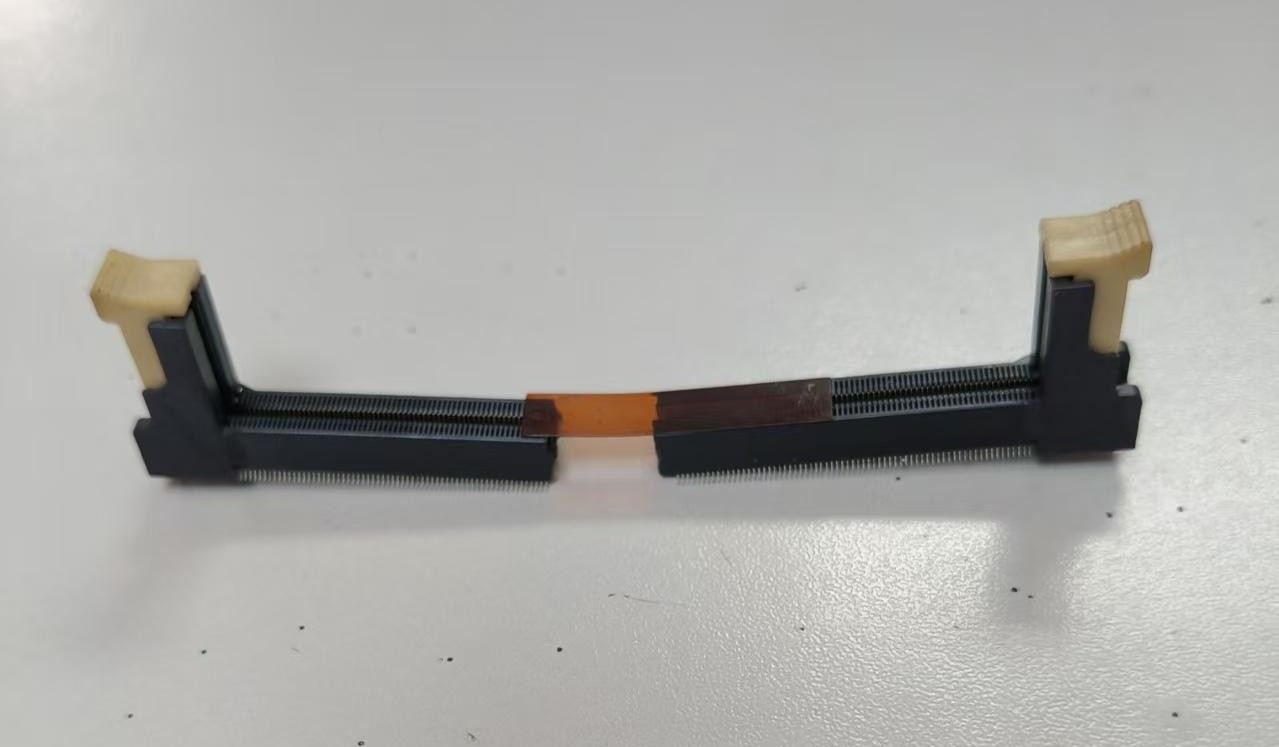
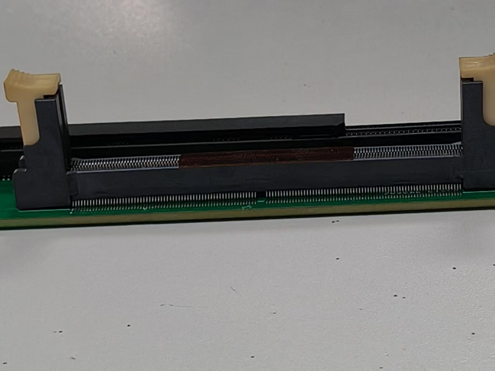
Turns out it is the (expensive) SODIMM that melted and scorched, not the UDIMM. The distributor says we need to pre-bake it, so we’ll try,but I’m not sure that will cut it.
2 Likes
Hmm, pre-baking is usually used against moisture. I haven’t heard that it also affects bending. But you never know.
Could it be that the upright version of the SO-DIMM is a bit uncommon of a form factor? SO-DIMM is mostly used in laptops and mini-pcs and they don’t have the height for this. So they mostly use sockets that hold the SO-DIMM horizontally.
Using these would mean a bigger plank pcb. But could on the other hand make sourcing the sockets easier.
2 Likes
You are correct. It is a specialty item. I will look at the more typical sockets, maybe there is something okay.
My concern about the laptop style socket is that they seems to be kind of weak and low life. A lot have that push down to click mechanism that terrifies me ![]()
2 Likes
With DDR5 you get a limited number of insertion cycles everywhere. But not because they break down, but because the proper impedance matching has quite narrow tolerances. But this isn’t of concern for a plank that is just about accessing the EEPROM.
I haven’t seen one of the retaining clips on the sides of a horizontal SO-DIMM socket actually break while the rest of the socket was still ok. But maybe you need some extra cushioning for shipping.
1 Like
Good insight on the impedance matching, thank you. I did not know that.
We’ve got a lead on two more vertical sockets, one from lotes and one from foxconn.
I also had a look at horizontal sockets and I’m willing to give it a try. Will find out more tomorrow AM China time.
1 Like

The shop with the sodimm socket lists two more now, a LOTES and a unknown. Both cheaper than captain melty. The LOTES isn’t actually available yet, but we got the unknown and it has the same footprint. The assembly should be done soon.
1 Like
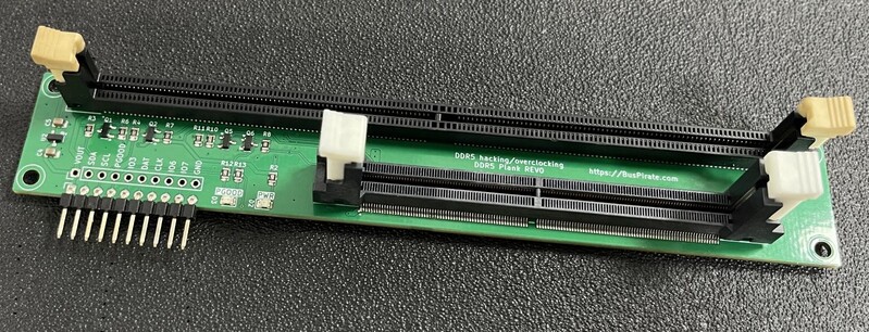
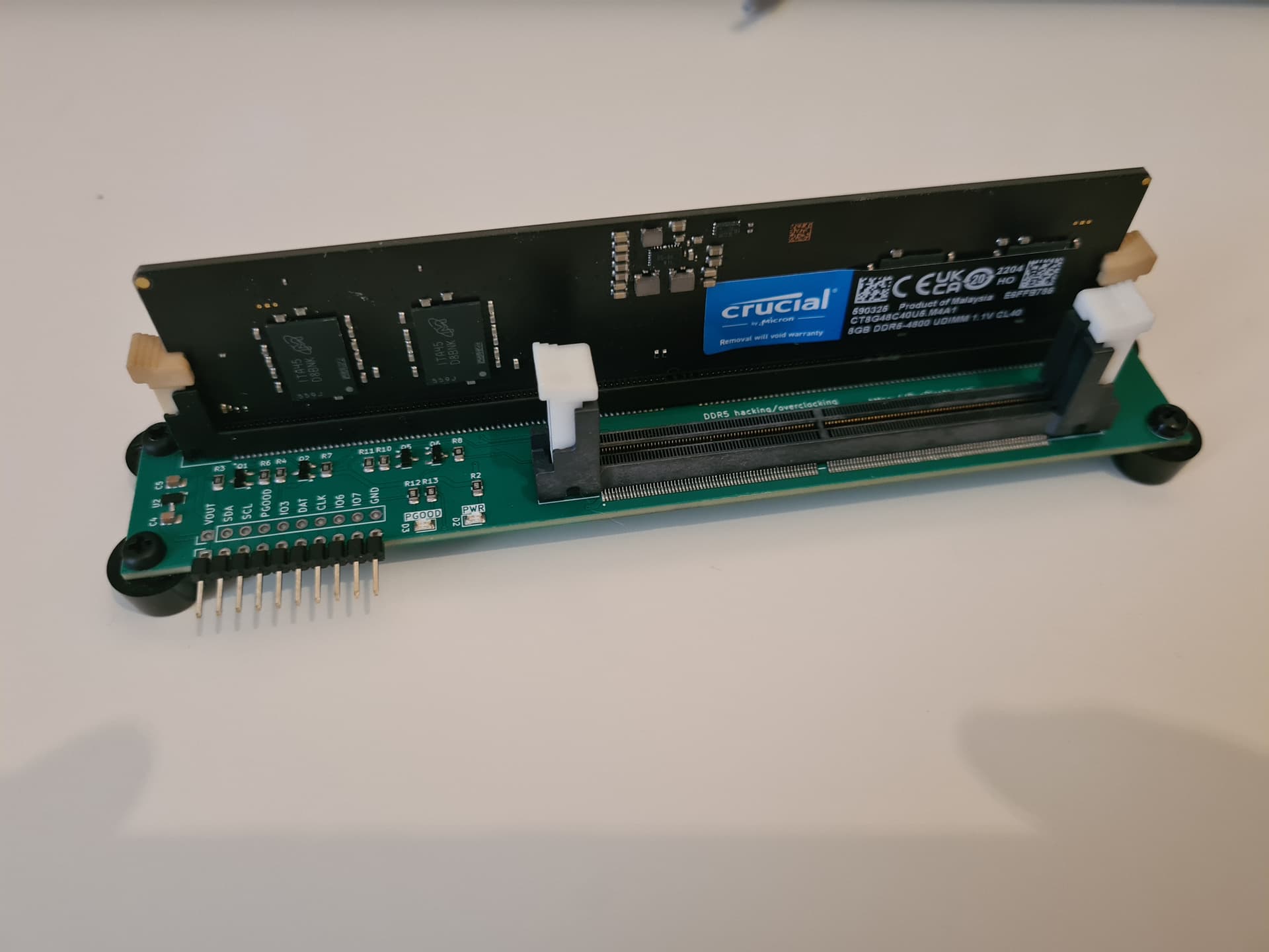
Finally got the reworked DDR5 board. Looks like The UDIMM got a bit cooked on the send pass through the reflow oven (maybe just the actual color?).
One is on the way to me, one is on the way to @electronic_eel.
First impressions:
- CLK and DAT on pin header is wrong, left over from a different board (think this is already fixed)
- Round the corners
- Without feeling it, I think it probably needs to be wider for stability.
- The PGOOD and PWR LEDs should swap places, in my mind that flows better.
Really looking forward to writing an analysis tool when I receive the board.
1 Like
Read the JEDEC documentation for DDR5 SPD last night. Make a big struct for it today. Very very excited for this board to arrive.
1 Like
Bug found, kind of
It looks like the bidirectional level shifter interacts with the Bus Pirate 5 series protection resistors in a way that can never achieve a proper low signal. I removed the redundant 5volt pull-up on the Bus Pirate side, but that wasn’t enough. Replacing the 2K resistor with 10K on the 3.3volt DDR5 side did the trick.
This did not effect Bus Pirate 6 or 7 which have smaller series resistors.
I also need to scope PWR_GOOD because I don’t think it’s working the way I understand the datasheet to describe.
Read and decode volatile memory (SPD settings)
Yikes this board took so long to get done that I forgot the details posted above.
There are two types of memory, volatile and non volatile.
- Volatile memory stores settings and values for the SPD chip itself, and follows the layout in the SPD docs linked above. Volatile memory is accessed when the MemReg bit is 0.
- Non volatile memory (the EEPROM) stores tables in accordance with JEDEC 5118, and is accessed when MemReg bit is 1.
There are two ways to access the different blocks of EEPROM:
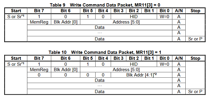
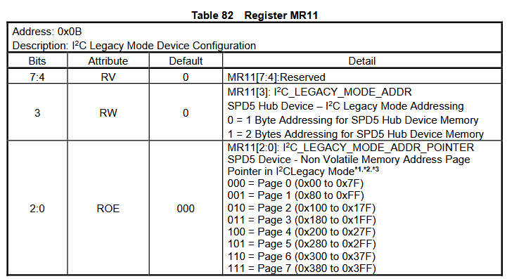
- Default I2C legacy mode (when MemReg 11 bit 3 =0), MemReg 11 bits 2:0 point to the active EEPROM page
- 2 byte address mode (When MemReg 11 bit 3 =1) where the block selection is packed into a second address byte.
In legacy mode MR11[2:0] select a 128 byte page. Each page consists of two 64 byte blocks.
I2C> [ 0xa0 0x0b [ 0xa1 r]

I2C START
TX: 0xA0 ACK 0x0B ACK
I2C REPEATED START
TX: 0xA1 ACK
RX: 0x00 NACK
I2C STOP
I2C>
Lets read MR11 to see what mode we’re in. The first bit (MemReg) of the MR11 address is 0 because it is volatile memory, then the address (11/0x0b). We get 0 so we’re in legacy mode I2C mode. Let’s stick with this so we don’t accidentally overwrite anything.
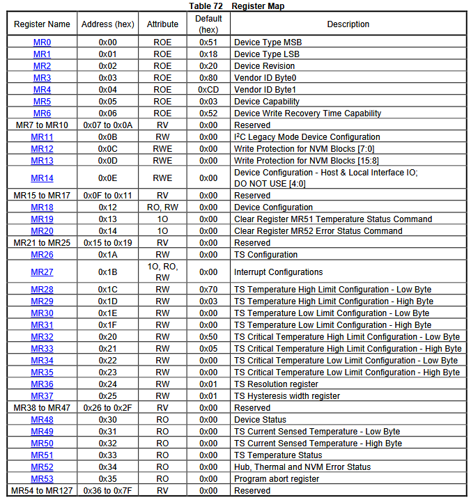
Here’s a register list for the volatile memory that configures the SPD chip.
I2C> ddr5
Device Type: 0x5118
Device Revision: 1.4
Vendor ID: 0x8632
Device Capability - Temperature Sensor Support: 1
Device Capability - Hub Support: 1
Write Recovery Time Capability: 3ms
I2C Legacy Mode Address Pointer Mode: 1 byte address
I2C Legacy Mode Address Pointer: page 0
Write Protection for NVM Blocks:
  Block 0: Protected
  Block 1: Protected
  Block 2: Protected
  Block 3: Protected
  Block 4: Protected
  Block 5: Protected
  Block 6: Protected
  Block 7: Protected
  Block 8: Protected
  Block 9: Protected
  Block 10: Unprotected
  Block 11: Unprotected
  Block 12: Unprotected
  Block 13: Unprotected
  Block 14: Unprotected
  Block 15: Unprotected
Device Configuration - Host & Local Interface IO: 0x00
Device Configuration: 0x00
Temp Sensor: Enabled
Interrupt Configurations: 0x00
TS Temperature High Limit: 0x0370
TS Temperature Low Limit: 0x0000
TS Critical Temperature High Limit: 0x0550
TS Critical Temperature Low Limit: 0x0000
TS Resolution: 9 bits
TS Hysteresis Width: 0x00
Device Status: 0x04
Device Status - Write Protect Override: Enabled
TS Current Sensed Temperature: 22.5c
TS Temperature Status: 0x00
Error Status: 0x00
Program Abort Register: Normal
Made a struct to decode the volatile memory info according to the table above.
Looks pretty good. No big surprises here. The main point of interest is probably the list of write protected blocks, if write protect is overridden (HSA pin to ground, the plank handles this), and perhaps the temperature.
Next we’ll read and decode the actual JEDEC 5118 DDR5 setting tables - exciting!
1 Like
I’m going to rework how we decode values. I think it’s important to give the raw value and then decode after. Either on the same line (revision, temperature) or as separate lines (device status, write protection, device capability).
This leaves some room for debugging the bus pirate code instead of locking users in with what ay be my incorrect interpretation.
1 Like
Updated to decode some of the first page of EEPROM values. Not going to do everything because it’s a lot. It might be nice to read out the manufacturer name info, which is on a different page.
I think the best next step is to dump the whole EEPROM to a file for analysis in a HEX editor. Then something to write (regions) of the EEPROM to rescue bricked sticks and write in manufacturer “extra data” used to lock devices to official RAM.
End of day update
I2C> ddr5
Device Type: 0x5118
Device Revision: 1.4
Vendor ID: 0x8632
Device Capability - Temperature Sensor Support: 1
Device Capability - Hub Support: 1
Write Recovery Time Capability: 3ms
I2C Legacy Mode Address Pointer Mode: 1 byte address
I2C Legacy Mode Address Pointer: page 0
Write Protection for NVM Blocks: 0x03FF
  Block 0: Protected
  Block 1: Protected
  Block 2: Protected
  Block 3: Protected
  Block 4: Protected
  Block 5: Protected
  Block 6: Protected
  Block 7: Protected
  Block 8: Protected
  Block 9: Protected
  Block 10: Unprotected
  Block 11: Unprotected
  Block 12: Unprotected
  Block 13: Unprotected
  Block 14: Unprotected
  Block 15: Unprotected
Device Configuration - Host & Local Interface IO: 0x00
Device Configuration: 0x00
Interrupt Configurations: 0x00
Device Status: 0x04
Device Status - Write Protect Override: Enabled
Temp Sensor: Enabled
TS Resolution: 9 bits
TS Hysteresis Width: 0x00
TS Current Sensed Temperature: 0x0164 (22.0c)
TS Temperature High Limit: 0x0370 (55.0c)
TS Temperature Low Limit: 0x0000 (0.0c)
TS Critical Temperature High Limit: 0x0550 (85.0c)
TS Critical Temperature Low Limit: 0x0000 (0.0c)
TS Temperature Status: 0x00
Error Status: 0x00
Program Abort Register: Normal
The SPD hub has a 128 byte register/volatile memory area. The most interesting bits are the block write protection status and the temperature control stuff.
EEPROM SPD Data blocks 0-7:
CRC verify
Stored CRC: 0x72CB
Calculated CRC: 0x72CB
CRC okay :)
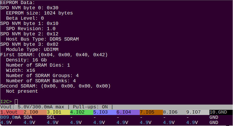
SPD NVM byte 2: 0x12
Host Bus Type: DDR5 SDRAM
SPD NVM byte 1: 0x10
SPD Revision: 1.0
SPD NVM byte 0: 0x30
EEPROM size: 1024 bytes
Beta Level: 0
SPD NVM byte 3: 0x02
Module Type: UDIMM
First SDRAM: (0x04, 0x00, 0x40, 0x42)
Density: 16 Gb
Number of SRAM Dies: 1
Width: x16
Number of SDRAM Groups: 4
Number of SDRAM Banks: 4
Second SDRAM: (0x00, 0x00, 0x00, 0x00)
Not present
DDR5 SPD has a 1024 byte EEPROM. The data is stored in 64 byte lockable blocks. There are 2 blocks to a page and 15 pages total.
The first 512 bytes is defined by the SDP 5118 spec. It contains info about the DDR RAM module. It ends with 2 checksum bytes, which the command now tests before processing.
EEPROM Manufacturing Information blocks 8-9:
Module Manuf. Code: 0x859B
Module Manuf. Location: 0x00
Module Manuf. Date: 22Y/04W
Module Serial Number: 0xE6FFB785
Module Part Number: CT8G48C40U5.M4A1

Module Revision Code: 0x57
DRAM Manuf. Code: 0x802C
DRAM Stepping: 0x41

Searching Manuf. Specific Data area block 9...

@ 0x22B: 0x34 0x35 0x31 0x30 0x39 0x30 0x34 0x38 0x31 0x39 0x00 0x00 0x00 0x00 0x00 0x00 0x00 0x00 0x00 0x00
The next two blocks (128 bytes) contains standardized manufacturer information. The end of block 9 from 0x22B to 0x27F contains optional manufacturer specific data. The command searches this space for non-zero values, then displays the values until there are 10 consecutive zero values indicating the likely end of data.
This is one place manufacturers might hide data that locks a machine to a specific authorized RAM stick.
Searching End User Programmable Area block 10-15...

@ 0x280: 0x0C 0x4A 0x30 0x01 0x01 0x80 0xB3 0x01 0x02 0x00 0x00 0x00 0x00 0x00 0x34 0x38 0x30 0x30 0x20 0x43 0x4C 0x34 0x30 0x20 0x20 0x20 0x20 0x20 0x20 0x20 0x00 0x00 0x00 0x00 0x00 0x00 0x00 0x00 0x00 0x00

@ 0x2BE: 0x25 0x34 0x30 0x22 0x22 0x00 0x22 0xA0 0x01 0x7A 0x0D 0x00 0x00 0x00 0x00 0x00 0x41 0x80 0x3E 0x80 0x3E 0x00 0x7D 0x80 0xBB 0x30 0x72 0x27 0x01 0xA0 0x00 0x82 0x00 0x00 0x00 0x00 0x00 0x00 0x00 0x00 0x00 0x00

@ 0x2FB: 0x03 0x02 0x00 0xA2 0x3E 0x00 0x00 0x00 0x00 0x00 0x00 0x00 0x00 0x00 0x00
The remainder of the EEPROM is “End User Programmable” and should be blank. However, this is also where extended overclock profiles are stored for EXPO (AMD) and XTD (Intel) compatible RAM sticks.
This is another area unscrupulous manufacturers might hide data that locks a machine to a specific authorized RAM stick.
Next up: dump and burn!
3 Likes
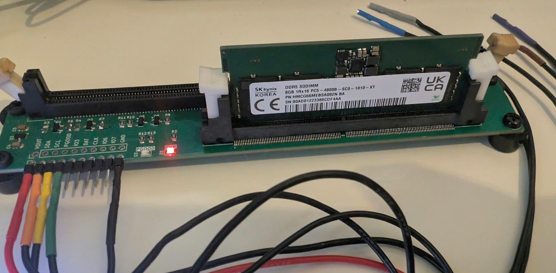
An e-Waste DDR5 SODIMM just popped through the mail slot.
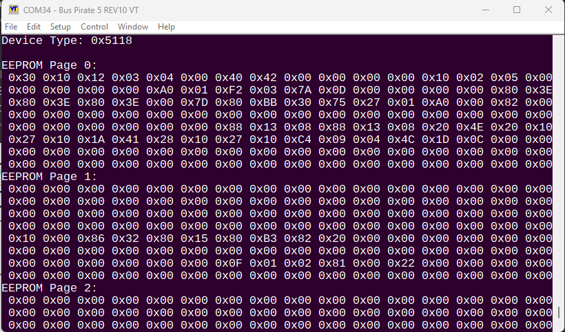
I2C> ddr5
Device Type: 0x5118
Device Revision: 1.5
Vendor ID: 0x8632
Device Capability - Temperature Sensor Support: 1
Device Capability - Hub Support: 1
Write Recovery Time Capability: 3ms
I2C Legacy Mode Address Pointer Mode: 1 byte address
I2C Legacy Mode Address Pointer: page 0
Write Protection for NVM Blocks: 0x01FF
  Block 0: Protected
  Block 1: Protected
  Block 2: Protected
  Block 3: Protected
  Block 4: Protected
  Block 5: Protected
  Block 6: Protected
  Block 7: Protected
  Block 8: Protected
  Block 9: Unprotected
  Block 10: Unprotected
  Block 11: Unprotected
  Block 12: Unprotected
  Block 13: Unprotected
  Block 14: Unprotected
  Block 15: Unprotected
Device Configuration - Host & Local Interface IO: 0x00
Device Configuration: 0x00
Interrupt Configurations: 0x00
Device Status: 0x04
Device Status - Write Protect Override: Enabled
Temp Sensor: Enabled
TS Resolution: 9 bits
TS Hysteresis Width: 0x00
TS Current Sensed Temperature: 0x0164 (22.0c)
TS Temperature High Limit: 0x0370 (55.0c)
TS Temperature Low Limit: 0x0000 (0.0c)
TS Critical Temperature High Limit: 0x0550 (85.0c)
TS Critical Temperature Low Limit: 0x0000 (0.0c)
TS Temperature Status: 0x00
Error Status: 0x00
Program Abort Register: Normal
Same SPD chip vendor ID (how to look that up? we have a JEDEC list in the firmware for flash chips, but I don’t know how to use it). Different device revision.
Interestingly page 9, which is a standardized manufacturer info block, is not protected on the stick.
EEPROM SPD Data blocks 0-7:

CRC verify
Stored CRC: 0x3E37
Calculated CRC: 0x3E37
CRC okay :)

SPD bytes 0-3: 0x30, 0x10, 0x12, 0x03
  Host Bus Type: DDR5 SDRAM
  SPD Revision: 1.0
  EEPROM size: 1024 bytes
  Beta Level: 0
  Module Type: SODIMM
First SDRAM: (0x04, 0x00, 0x40, 0x42)
  Density: 16 Gb
  Number of SRAM Dies: 1
  Width: x16
  Number of SDRAM Groups: 4
  Number of SDRAM Banks: 4
Second SDRAM: (0x00, 0x00, 0x00, 0x00)
  Not present
Everything is about the same.
EEPROM Manufacturing Information blocks 8-9:
Module Manuf. Code: 0x80AD
Module Manuf. Location: 0x01
Module Manuf. Date: 22Y/33W
Module Serial Number: 0x86CDF4AA
Module Part Number: HMCG66MEBSA092N

Module Revision Code: 0x00
DRAM Manuf. Code: 0x80AD
DRAM Stepping: 0xFF
The serial and part number are consistent with the label. Different DRAM chip manufacturer (again, how to use the JEDEC list to get the name?).
Searching Manuf. Specific Data area block 9:

@ 0x22C: 0x54 0x48 0x42 0x38 0x4E 0x36 0x36 0x31 0x36 0x32 0x30 0x32 0x00 0x00 0x00 0x00 0x00 0x00 0x00 0x00 0x01 0x00 0x21 0x00 0x00 0x00 0x00 0x00 0x00 0x00 0x00 0x00 0x00

Searching End User Programmable Area blocks 10-15:
Only a tiny bit of custom data in the Manufac. Specific Data area, none in the EUP area.
I’ve started to transfer this thread to a tutorial in docs, when it is in decent draft form I’ll push it to the live site.
Now that we’ve verified that the plank is working, I’ll make a few tweaks for REV1, which will probably be the first production board.
1 Like
Massive cleanup/reorg of the spaghetti code. Dumping works, but not yet to a file.
Pushed the ddr5 command to main, so it should be available in the firmware if anyone wants to check it out. It won’t do much without a DDR5 stick connected though.
1 Like
Maybe some safety precautions that its not hot-swapable when power is on? I guess piips know but better safe than sorry
2 Likes
If that would only fry the inserted chip, that seems a reasonable risk.
If ejection with power would fry the buspirate… how much cost does it add to prevent that?
2 Likes
In my experience the inrush from swapping sticks causes the bus pirate current limit fuse to blow. The PMIC has a bunch of inductors and caps, and most seem to make a big deal about how fast they get up to voltage so the start current is pretty impressive.
It’s really interesting how they gave up on motherboard wide voltage distribution and put the supply directly on the ram stick. It reduces the pins needed to power the stick, worry about noisy parts on the MB is basically eliminated. New evolutions of DDR ram chips can just swap in the new values for the PMIC without a full motherboard architecture change.
I don’t know, but I would assume PCIE is basically going the same direction with onboard PMICs and a 12 or 5 volt supply to the card.
1 Like
Everything but writing, and man it is a mess! There will be some hours of cleanup and overall storage code rework when this is done…
I2C> ddr5 read -f ddr5.bin
Read SPD NVM to file: ddr5.bin
Wrote 128 bytes to file ddr5.bin
Wrote 128 bytes to file ddr5.bin
Wrote 128 bytes to file ddr5.bin
Wrote 128 bytes to file ddr5.bin
Wrote 128 bytes to file ddr5.bin
Wrote 128 bytes to file ddr5.bin
Wrote 128 bytes to file ddr5.bin
Wrote 128 bytes to file ddr5.bin
Successfully read SPD NVM to file: ddr5.bin

I2C>
Dump DDR5 SPD NVM to a file.
I2C> ddr5 crc -f ddr5.bin
Checking CRC for JEDEC blocks 0-7, file: ddr5.bin

CRC verify
Stored CRC (bytes 510:511): 0x37 0x3E
Calculated CRC: 0x16 0x2E
Error: CRC does not match!!!
Verify (or calculate after changes) the CRC in a NVM dump file.
I2C> ddr5 verify -f ddr5.bin
Verifying SPD NVM against file: ddr5.bin
Error: SPD NVM byte 125 does not match file! (0x01 != 0x00)
Verification failed, SPD NVM does not match file ddr5.bin

I2C>
Verify DDR5 SPD NVM contents against a dump file.
I2C> ddr5 lock
Device Type: 0x5118
 Block| Old State | New State
------|-----------|-----------
  0   | Locked | Locked
  1   | Locked | Locked
  2   | Locked | Locked
  3   | Locked | Locked
  4   | Locked | Locked
  5   | Locked | Locked
  6   | Locked | Locked
  7   | Locked | Locked
  8   | Locked | Locked
  9   | Locked | Locked
  10   | Unlocked | Unlocked
  11   | Unlocked | Unlocked
  12   | Unlocked | Unlocked
  13   | Unlocked | Unlocked
  14   | Unlocked | Unlocked
  15   | Unlocked | Unlocked
Show block lock states.
I2C> ddr5 lock -b 15
Locking NVM block 15
Device Type: 0x5118
Lock bits set successfully: 0xFF 0x83
 Block| Old State | New State
------|-----------|-----------
  0   | Locked | Locked
...
  15   | Unlocked | Locked
I2C> ddr5 unlock -b 15
Unlocking NVM block 15
Device Type: 0x5118
Lock bits set successfully: 0xFF 0x03
 Block| Old State | New State
------|-----------|-----------
  0   | Locked | Locked
...
  15   | Locked | Unlocked
Lock and unlock NVM blocks.
1 Like