Got a wonderful package today. Inside was the prototype board.
Board layout was fine
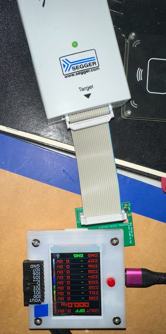
As can be seen, the orientation of the 20-pin header is correct. The key on the cable’s connector is facing AWAY from the buspirate. So, with a shroud, the slot would also be on the side furthest from the three debug pins. This is all as expected.
Connected and found the device
SEGGER J-Link Commander V8.10f (Compiled Nov  6 2024 16:15:11)
DLL version V8.10f, compiled Nov  6 2024 16:12:18

Connecting to J-Link via USB...O.K.
Firmware: J-Link V10 compiled Jan 30 2023 11:28:07
Hardware version: V10.10
J-Link uptime (since boot): N/A (Not supported by this model)
S/N: *********
License(s): FlashBP, GDB
OEM: ******
VTref=3.300V (fixed)


Type "connect" to establish a target connection, '?' for help
J-Link>connect
Please specify device / core. <Default>: RP2040_M0_0
Type '?' for selection dialog
Device>
Please specify target interface:
  J) JTAG (Default)
  S) SWD
  T) cJTAG
TIF>S
Specify target interface speed [kHz]. <Default>: 4000 kHz
Speed>
Device "RP2040_M0_0" selected.


Connecting to target via SWD
ConfigTargetSettings() start
J-Link script: ConfigTargetSettings()
ConfigTargetSettings() end - Took 213us
Found SW-DP with ID 0x0BC12477
DPIDR: 0x0BC12477
CoreSight SoC-400 or earlier
Scanning AP map to find all available APs
AP[1]: Stopped AP scan as end of AP map has been reached
AP[0]: AHB-AP (IDR: 0x04770031, ADDR: 0x00000000)
Iterating through AP map to find AHB-AP to use
AP[0]: Core found
AP[0]: AHB-AP ROM base: 0xE00FF000
CPUID register: 0x410CC601. Implementer code: 0x41 (ARM)
Found Cortex-M0 r0p1, Little endian.
FPUnit: 4 code (BP) slots and 0 literal slots
CoreSight components:
ROMTbl[0] @ E00FF000
[0][0]: E000E000 CID B105E00D PID 000BB008 SCS
[0][1]: E0001000 CID B105E00D PID 000BB00A DWT
[0][2]: E0002000 CID B105E00D PID 000BB00B FPB
Memory zones:
  Zone: "Default" Description: Default access mode
Cortex-M0 identified.
J-Link>
Other thoughts
Not recommended for use on flat surface without more. The edge of the buspirate with the USB port in my case was ~7mm off the flat surface. This put stress on the debug pins (and one bent). The pins having those large metal standoffs raised the height of the BP5. Definitely needs support.
I expect I’ll layer a few pieces of EVA foam, with cutouts for the PCB which will both lift the buspirate, and give me something to cut holes in when the new cases arrive so the feet don’t impact this. so that the buspirate can have a stable surface to rest on. Maybe I’ll even add some corner cutouts / guides in EVA foam, to make it trivial to align.
Recommended revisions:
- Shrouded, keyed header; key slot on side furthest from debug pins (yes, I know it’s already plan-of-record)
- Can the final PCB have an oversized hole for the foot of the new case’s to rest in? This will help a single “holder” support both the old and new cases.
- Fit’n’Finish … it’s a small thing … Can the corners of the PCB have rounded edges? Sharp corners are fine for the prototype, but even a few mm rounding would greatly improve.
- Luxury … So much PCB just begging for nice silkscreen art. Maybe the BP logo guy on the bottom?
Thanks for this! I will play around with some foam + manual cuts + rubber cement, see if I come up with anything reasonable as a “drop in” alignment helper / support structure.